1. What is FIFO
FIFO is a first in first out data buffer, which is widely used in logic design. FIFO design can be said to be a common sense design that logic designers must master. FIFO is generally used to isolate places where the read-write bandwidth on both sides is inconsistent or the bit width is different. In FPGA design, there are generally two methods to use FIFO. The first method is to directly call the official FIFO IP, and the other method is to design FIFO control logic by yourself. Of course, when we learn to design FIFO, we don't really need to make our own wheels. It just means that as practitioners, we need to understand the relevant design methods. After all, our own wheels don't necessarily run.
FIFO includes synchronous FIFO and asynchronous FIFO. Synchronous FIFO has a clock signal, which is used by read and write logic. Asynchronous FIFO has two clock signals, which are used by read and write logic. The difference between FIFO and ordinary memory RAM is that there is no external read-write address line, which is very simple to use, but the disadvantage is that it can only write data in sequence. The data address is automatically added by 1 by the internal read-write pointer. It can not be read or written to a specified address by the address line like ordinary memory. FIFO is essentially a FIFO data buffer composed of ram and read-write control logic.
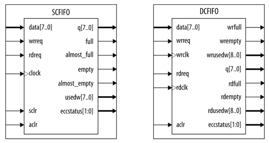
Common parameters of FIFO:
- FIFO width: that is, the data bits of FIFO for one read / write operation
- Depth of FIFO: refers to how many N-bit data can be stored in FIFO (if the width is N)
- Full flag: a signal sent by the FIFO state when the FIFO is full or about to be full to prevent the FIFO write operation from continuing to write data to the FIFO, resulting in overflow
- Empty flag: a signal sent by the FIFO state when the FIFO is empty or about to be empty, so as to prevent the reading operation of FIFO from continuing to read data from FIFO, resulting in the reading of invalid data (underflow)
- Read clock: the clock followed by the read operation. Data is read at each clock edge (consistent with the write clock in the synchronization FIFO)
- Write clock: the clock followed by the write operation. Data is written at each clock edge (consistent with the read clock in the synchronization FIFO)
2. Design method of synchronous FIFO
Working principle of FIFO read-write pointer (read-write pointer is read-write address):
- Write pointer: always point to the next unit to be written. When reset, point to the first unit (No. 0)
- Read pointer: it always points to the data to be read out. During reset, it points to the "empty" / "full" detection of the first unit (No. 0) FIFO
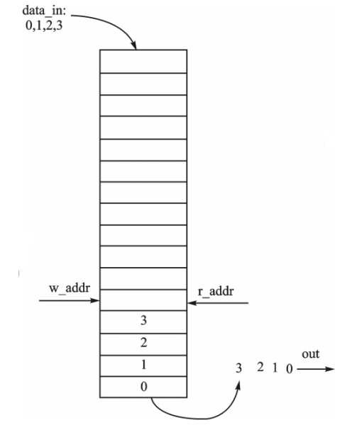
The key of FIFO design is to generate reliable FIFO read-write pointer and FIFO "empty" / "full" status flag. When the read-write pointers are equal, it indicates that the FIFO is empty. This occurs during the reset operation, or when the read pointer catches up with the write pointer after reading the last word in the FIFO, as shown in the following figure:
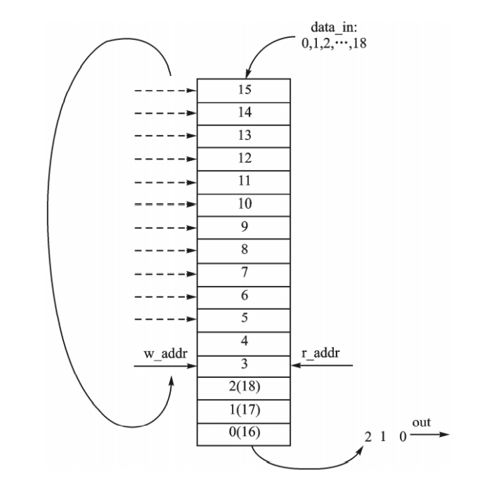
When the read-write pointers are equal again, it indicates that the FIFO is full. This happens when the write pointer rotates one circle and the wrapped around catches up with the read pointer, as shown in the following figure:
It can be seen that the read-write pointer can be + 1 per clock cycle when the read-write enable is effective, and how to generate a reliable "empty" / "full" signal has become the focus of synchronous FIFO design. There are two solutions:
2.1 counter method
Build a counter (fifo_cnt) to indicate the number of data in the current FIFO:
- When reset, the counter is 0 and the number of data in FIFO is 0
- When the read / write enable signals are valid, it means that the counter is read and write again, the counter remains unchanged, and the number of data in FIFO does not change
- When write enable is valid and full=0, fifo_cnt +1; Indicates that when a write operation occurs and the FIFO is not full, the number of data in the FIFO increases by 1
- When the read enable is valid and empty=0, fifo_cnt -1;; Indicates that the number of data in the FIFO is reduced by 1 when the FIFO is not full
- fifo_ When CNT = 0, it means that FIFO is empty and empty=1 needs to be set; fifo_ CNT = depth of FIFO When, it means that the FIFO is now full and full=1 needs to be set
2.1.1 Verilog code
After solving the above problems, you can easily post Verilg Code:
//Realization of synchronous FIFO by counter method
module	sync_fifo_cnt
#(
	parameter   DATA_WIDTH = 'd8  ,							//FIFO bit width
    parameter   DATA_DEPTH = 'd16 							//FIFO depth
)
(
	input									clk		,		//System clock
	input									rst_n	,       //Low level active reset signal
	input	[DATA_WIDTH-1:0]				data_in	,       //Data written
	input									rd_en	,       //Read enable signal, high level active
	input									wr_en	,       //Write enable signal, high level active

	output	reg	[DATA_WIDTH-1:0]			data_out,	    //Output data
	output									empty	,	    //Empty flag, high level indicates that the current FIFO is full
	output									full	,       //Full flag, high level indicates that the current FIFO has been read empty
	output	reg	[$clog2(DATA_DEPTH) : 0]	fifo_cnt		//$clog2 is the base 2 logarithm
);

//reg define
reg [DATA_WIDTH - 1 : 0] fifo_buffer[DATA_DEPTH - 1 : 0];	//Implementation of RAM with two-dimensional array
reg [$clog2(DATA_DEPTH) - 1 : 0]	wr_addr;				//Write address
reg [$clog2(DATA_DEPTH) - 1 : 0]	rd_addr;				//Read address

//Read operation, update read address
always @ (posedge clk or negedge rst_n) begin
	if (!rst_n)
		rd_addr <= 0;
	else if (!empty && rd_en)begin							//The read enable is valid and not empty
		rd_addr <= rd_addr + 1'd1;
		data_out <= fifo_buffer[rd_addr];
	end
end
//Write operation, update write address
always @ (posedge clk or negedge rst_n) begin
	if (!rst_n)
		wr_addr <= 0;
	else if (!full && wr_en)begin							//Write enable is valid and not full
		wr_addr <= wr_addr + 1'd1;
		fifo_buffer[wr_addr]<=data_in;
	end;
end
//Update counter
always @ (posedge clk or negedge rst_n) begin
	if (!rst_n)
		fifo_cnt <= 0;
	else begin
		case({wr_en,rd_en})									//Splicing read-write enable signal for judgment
			2'b00:fifo_cnt <= fifo_cnt;						//No reading, no writing
			2'b01:	                               			//Just read
				if(fifo_cnt != 0)				   			//fifo is not read empty
					fifo_cnt <= fifo_cnt - 1'b1;   			//Number of fifo - 1
			2'b10:                                 			//Just write
				if(fifo_cnt != DATA_DEPTH)         			//fifo is not full
					fifo_cnt <= fifo_cnt + 1'b1;   			//Number of fifo + 1
			2'b11:fifo_cnt <= fifo_cnt;	           			//Simultaneous reading and writing
			default:;
		endcase
	end
end
//Update the indication signal according to the counter status
//According to different thresholds, you can also design half empty, half full, almost empty and almost full
assign full  = (fifo_cnt == DATA_DEPTH) ? 1'b1 : 1'b10;		//Null signal
assign empty = (fifo_cnt == 0)? 1'b1 : 1'b0;				//Full signal

endmodule
2.1.2 Testbench and simulation results
Next, write a script to test the source code:
- Instantiate a synchronous FIFO with a depth of 8 and a bit width of 8
- Write FIFO first until it is full, and the written data is random data
- Then read the FIFO until it is empty
- Then write four random data to FIFO and read them at the same time
`timescale 1ns/1ns	//Time unit / precision

//------------< module and Port declaration >----------------------------------------
module tb_sync_fifo_cnt();

parameter   DATA_WIDTH = 8  ;			//FIFO bit width
parameter   DATA_DEPTH = 8 ;			//FIFO depth

reg									clk		;
reg									rst_n	;
reg		[DATA_WIDTH-1:0]			data_in	;
reg									rd_en	;
reg									wr_en	;

wire	[DATA_WIDTH-1:0]			data_out;
wire								empty	;
wire								full	;
wire	[$clog2(DATA_DEPTH) : 0]	fifo_cnt;


//------------< instantiate the module under test >----------------------------------------
sync_fifo_cnt
#(
	.DATA_WIDTH	(DATA_WIDTH),			//FIFO bit width
    .DATA_DEPTH	(DATA_DEPTH)			//FIFO depth
)
sync_fifo_cnt_inst(
	.clk		(clk		),
	.rst_n		(rst_n		),
	.data_in	(data_in	),
	.rd_en		(rd_en		),
	.wr_en		(wr_en		),

	.data_out	(data_out	),
	.empty		(empty		),
	.full		(full		),
	.fifo_cnt	(fifo_cnt	)
);

//------------< set initial test conditions >----------------------------------------
initial begin
	clk = 1'b0;							//The initial clock is 0
	rst_n <= 1'b0;						//Initial reset
	data_in <= 'd0;
	wr_en <= 1'b0;
	rd_en <= 1'b0;
//Repeat the write operation 8 times to fill the FIFO
	repeat(8) begin
		@(negedge clk)begin
			rst_n <= 1'b1;
			wr_en <= 1'b1;
			data_in <= $random;			//Generate 8-bit random number
		end
	end
//Repeat the read operation for 8 times to make the FIFO read empty
	repeat(8) begin
		@(negedge clk)begin
			wr_en <= 1'b0;
			rd_en <= 1'd1;
		end
	end
//Repeat the write operation for 4 times and write 4 random data
	repeat(4) begin
		@(negedge clk)begin
			wr_en <= 1'b1;
			data_in <= $random;	//Generate 8-bit random number
			rd_en <= 1'b0;
		end
	end
//Continuously read and write FIFO at the same time, and the written data is random data
	forever begin
		@(negedge clk)begin
			wr_en <= 1'b1;
			data_in <= $random;	//Generate 8-bit random number
			rd_en <= 1'b1;
		end
	end
end

//------------< set clock >----------------------------------------------
always #10 clk = ~clk; 			// System clock cycle 20ns

endmodule
modelsim is used for simulation, and the simulation results are as follows:
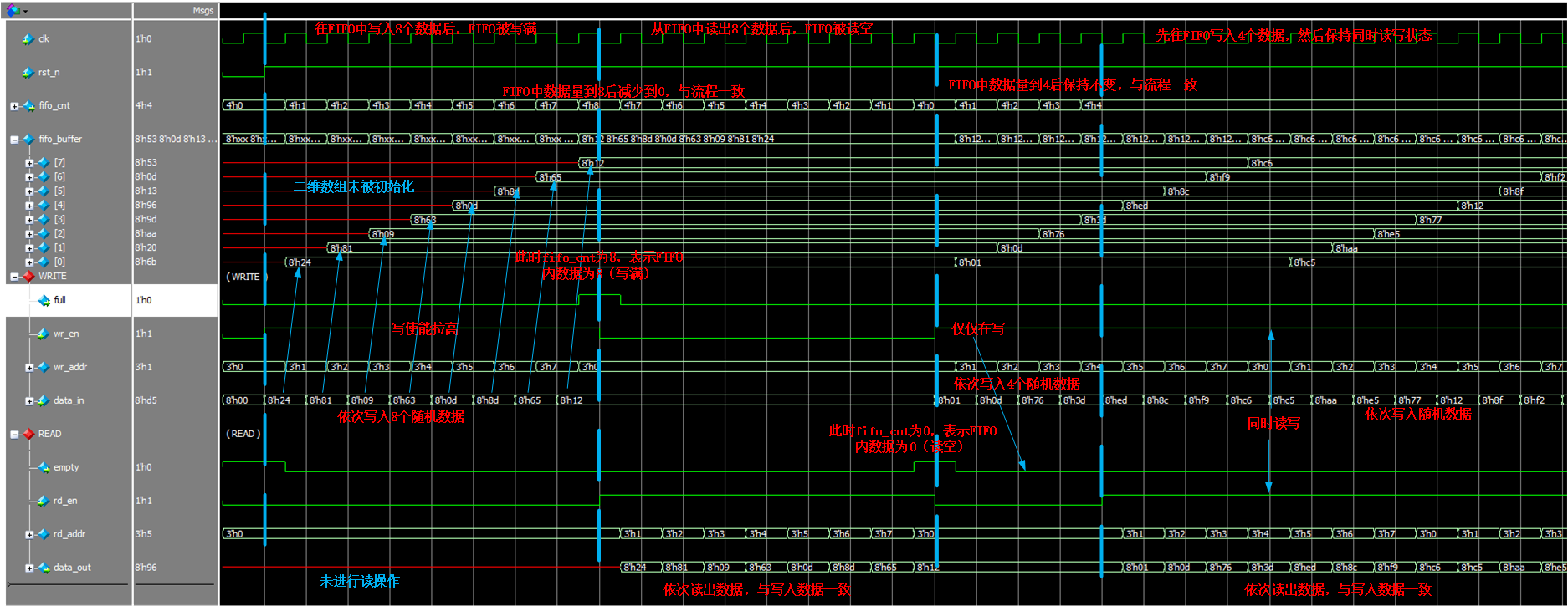 It can be seen that the simulation result is consistent with the expected effect (see the note in the figure for details).
2.2 high level expansion method
For example, in a FIFO with a depth of 8, a 3-bit read-write pointer is required to indicate the 8 addresses of the read-write addresses 3'b000-3'b111 respectively. If the address pointer is extended by 1 bit, it becomes a 4-bit address, and the address representation interval becomes 4'b0000-4'b1111. If you do not look at the highest bit, the representation interval of the last three bits is still 3'b000-3'b111, which means that the highest bit can be used as an indicator bit.
- When the highest bits are different and the other bits are the same, it means that the read pointer or write pointer has run one more circle, but obviously it will not let the read pointer run one more circle (what do you read by running one more circle?), so the possible situation can only be that the write pointer runs one more circle, and means that the FIFO is full
- When the highest bits are the same and the other bits are the same, it means that the read pointer has caught up with the write pointer or the write pointer has caught up with the read pointer, and obviously the write pointer will not catch up with the read pointer (in this case, the write pointer can only exceed the read pointer by one circle), so the possible situation can only be that the read pointer has caught up with the write pointer, which means that the FIFO is read empty
2.2.1 Verilog code
After solving the above problems, you can easily post Verilg Code:
module	sync_fifo_ptr
#(
	parameter   DATA_WIDTH = 'd8  ,								//FIFO bit width
    parameter   DATA_DEPTH = 'd16 								//FIFO depth
)
(
	input										clk		,		//System clock
	input										rst_n	,       //Low level active reset signal
	input	[DATA_WIDTH-1:0]					data_in	,       //Data written
	input										rd_en	,       //Read enable signal, high level active
	input										wr_en	,       //Write enable signal, high level active

	output	reg	[DATA_WIDTH-1:0]				data_out,	    //Output data
	output										empty	,	    //Empty flag, high level indicates that the current FIFO is full
	output										full		    //Full flag, high level indicates that the current FIFO has been read empty
);

//reg define
//Implementation of RAM with two-dimensional array
reg [DATA_WIDTH - 1 : 0]			fifo_buffer[DATA_DEPTH - 1 : 0];
reg [$clog2(DATA_DEPTH) : 0]		wr_ptr;						//Write address pointer, one more bit wide
reg [$clog2(DATA_DEPTH) : 0]		rd_ptr;						//Read address pointer, one bit wider

//wire define
wire [$clog2(DATA_DEPTH) - 1 : 0]	wr_ptr_true;				//Real write address pointer
wire [$clog2(DATA_DEPTH) - 1 : 0]	rd_ptr_true;				//Real read address pointer
wire								wr_ptr_msb;					//Write address pointer address highest bit
wire								rd_ptr_msb;					//Read address pointer address highest bit

assign {wr_ptr_msb,wr_ptr_true} = wr_ptr;						//Splice the highest bit with other bits
assign {rd_ptr_msb,rd_ptr_true} = rd_ptr;						//Splice the highest bit with other bits

//Read operation, update read address
always @ (posedge clk or negedge rst_n) begin
	if (rst_n == 1'b0)
		rd_ptr <= 'd0;
	else if (rd_en && !empty)begin								//The read enable is valid and not empty
		data_out <= fifo_buffer[rd_ptr_true];
		rd_ptr <= rd_ptr + 1'd1;
	end
end
//Write operation, update write address
always @ (posedge clk or negedge rst_n) begin
	if (!rst_n)
		wr_ptr <= 0;
	else if (!full && wr_en)begin								//Write enable is valid and not full
		wr_ptr <= wr_ptr + 1'd1;
		fifo_buffer[wr_ptr_true] <= data_in;
	end
end

//Update indication signal
//When all bits are equal, the read pointer catches the write pointer, and the FIFO is read null
assign	empty = ( wr_ptr == rd_ptr ) ? 1'b1 : 1'b10;
//When the highest bits are different but the other bits are equal, the write pointer exceeds the read pointer by one circle, and the FIFO is written empty
assign	full  = ( (wr_ptr_msb != rd_ptr_msb ) && ( wr_ptr_true == rd_ptr_true ) )? 1'b1 : 1'b0;

endmodule
2.2.2 Testbench and simulation results
Next, write a script to test the source code (consistent with 2.1.2):
- Instantiate a synchronous FIFO with a depth of 8 and a bit width of 8
- Write FIFO first until it is full, and the written data is random data
- Then read the FIFO until it is empty
- Then write four random data to FIFO and read them at the same time
`timescale 1ns/1ns	//Time unit / precision

//------------< module and Port declaration >----------------------------------------
module tb_sync_fifo_ptr();

parameter   DATA_WIDTH = 8  ;		//FIFO bit width
parameter   DATA_DEPTH = 8 ;		//FIFO depth

reg									clk		;
reg									rst_n	;
reg		[DATA_WIDTH-1:0]			data_in	;
reg									rd_en	;
reg									wr_en	;

wire	[DATA_WIDTH-1:0]			data_out;
wire								empty	;
wire								full	;
wire	[$clog2(DATA_DEPTH) : 0]	fifo_cnt;


//------------< instantiate the module under test >----------------------------------------
sync_fifo_ptr
#(
	.DATA_WIDTH	(DATA_WIDTH),			//FIFO bit width
    .DATA_DEPTH	(DATA_DEPTH)			//FIFO depth
)
sync_fifo_ptr_inst(
	.clk		(clk		),
	.rst_n		(rst_n		),
	.data_in	(data_in	),
	.rd_en		(rd_en		),
	.wr_en		(wr_en		),

	.data_out	(data_out	),
	.empty		(empty		),
	.full		(full		)
);

//------------< set initial test conditions >----------------------------------------
initial begin
	clk = 1'b0;					//The initial clock is 0
	rst_n <= 1'b0;				//Initial reset
	data_in <= 'd0;
	wr_en <= 1'b0;
	rd_en <= 1'b0;
//Repeat the write operation 8 times to fill the FIFO
	repeat(8) begin
		@(negedge clk)begin
			rst_n <= 1'b1;
			wr_en <= 1'b1;
			data_in <= $random;	//Generate 8-bit random number
		end
	end
//Repeat the read operation for 8 times to make the FIFO read empty
	repeat(8) begin
		@(negedge clk)begin
			wr_en <= 1'b0;
			rd_en <= 1'd1;
		end
	end
//Repeat the write operation for 4 times and write 4 random data
	repeat(4) begin
		@(negedge clk)begin
			wr_en <= 1'b1;
			data_in <= $random;	//Generate 8-bit random number
			rd_en <= 1'b0;
		end
	end
//Continuously read and write FIFO at the same time, and the written data is random data
	forever begin
		@(negedge clk)begin
			wr_en <= 1'b1;
			data_in <= $random;	//Generate 8-bit random number
			rd_en <= 1'b1;
		end
	end
end

//------------< set clock >----------------------------------------------
always #10 clk = ~clk; 			// System clock cycle 20ns

endmodule
modelsim is used for simulation, and the simulation results are as follows:
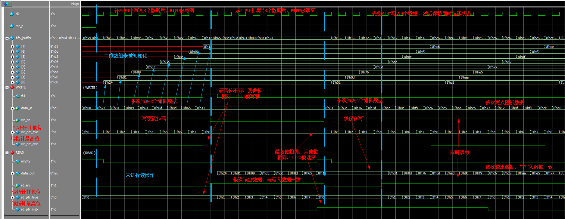
It can be seen that the simulation result is consistent with the expected effect (see the note in the figure for details).
3. Other
- After understanding the design method of synchronous FIFO, it is relatively simple to design asynchronous FIFO, which mainly solves the problem of cross clock domain comparison of read and write pointers in asynchronous FIFO. The next article will analyze and verify the design of asynchronous FIFO
- Friends who need the whole project can leave a private letter or comment in the email
- It's not easy to create. I hope you guys can support it for three times! If there is any mistake, please correct it!