preface
The previous article introduced various electrical standards related to the serial port. The last article mainly introduced how to use Verilog language to complete the serial port receiving function. This article mainly introduced how to complete the serial port sending function, and included a flexible check bit design. In the process of querying data in the early stage Black gold power community - blog Park Also found the relevant knowledge about this part, which also gives the design source code, detailed code explanation, interested friends can check it. [serial] [FPGA black gold development board] Verilog HDL - serial port module (11) . By reading the explanation of this article, I have a further understanding of Verilog language and a deeper understanding of the design format of the project. The main purpose of this article is to record the learning process and facilitate subsequent reference.
1, Serial communication protocol?
The information about the communication protocol of serial port is in the last article 2021-7-29 Verilog language realizes the transceiver receiving function of serial port (including flexible check bit design) I have explained it in detail. I won't repeat it here. Friends who are interested or don't know much can click to have a look. Some basic knowledge is more important, such as the basic functions of start bit and stop bit, as well as the knowledge related to baud rate and the basic method of baud rate calculation.
Compared with the receiving module, the transmitting module is simpler. The kernel of the receiving module is like "timing" reception, while the kernel of the sending module is "timing transmission". Compared with the receiving module, it also detects a start signal, that is, the detection of the falling edge at the beginning of the start bit mentioned in the previous article. However, compared with the transmission module, this part is no longer needed. It mainly completes the two functions of timing and transmission in timing transmission.
2, Modular design
This part still adopts the design scheme of sub module, which should be considered first. How to divide the modules? How can we divide the modules most reasonably and easily?
The functions we want to complete are 1 Timing 2 send out. If the timing is a module, it is equivalent to the generation of baud rate. Transmission is another module, which is equivalent to controlling the part of transmitting data.
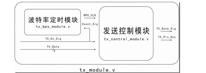
From the previous article, we can know that the timing module is a "encapsulated" counting module. That is, a counter. Is the counter counting? Of course not. Only when you decide to send data, you start counting, that is, timing, and stop counting after a frame of data is sent, that is, stop generating baud rate.
1. Baud rate design module
The content of this part is the same as the baud rate generation of the receiving module. The timing of timing reception and timing transmission is to generate a time interval. What to do after this interval is a follow-up control problem.
module tx_bps_module
(
	CLK,RSTn,
	Count_Sig,
	BPS_CLK,
);
	input CLK;
	input RSTn;
	input Count_Sig;
	output BPS_CLK;

	/*************************/

	reg [11:0] Count_BPS;

	always @ (posedge CLK or negedge RSTn )
		if(!RSTn)
			Count_BPS <= 12'd0;
		else if(Count_BPS == 12'd434)  //Timing 115200 bps
			Count_BPS <= 12'd0;
		else if(Count_Sig)             //Sending signal
			Count_BPS <= Count_BPS + 1'b1;
		else
			Count_BPS <= 12'd0;

	/*************************/

	assign BPS_CLK = (Count_BPS == 12'd217)? 1'b1 : 1'b0;  //Duration interval

	/*************************/

endmodule
It should be briefly mentioned here that in the receiving module, we design the middle bit, that is, 434 / 2 = 217, to read data in the middle, which is the most stable data. But why keep the same design in the sending module?
Here we are going to delve into the essence of the sending module. It is a regular transmission, that is, one data bit lasts for a certain time interval, and then another data bit is transmitted for a certain time interval. For example, it can be well understood.
Let's explain a figure in the previous article.
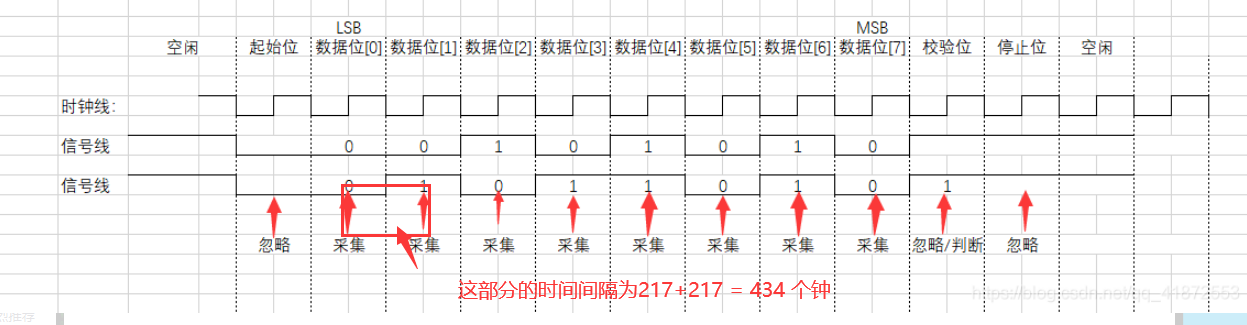
After a simple calculation, suppose that the baud rate of our serial port is set to 115200 bps and designed with 50 MHz.
In the last article, I introduced a formula, which can be used right now.
N = (1/BPS) / (1/F) = F / BPS
Of which:
N: Number of counts to be designed (rounded)
BPS: baud rate to be set for the designed serial port
F: The frequency of the dominant frequency used to count
We get N = 434. In other words, 434 50 MHz clocks are the time interval we want. OK. After a big circle, I still return to this time interval, that is, timing. Now we can understand that the generated high pulse signals also meet the interval of 434 minutes, which is the time interval required for this timing. This is the essence of baud rate generation in the transmission module.
2. Send data control module
With the generation of baud rate, it is now necessary to control the value of each bit in a frame of data. Here we still need to review the communication protocol.
- Idle state: high level
- Start bit: the time to pull down and last one bit, that is, the time to last 1/bps
- Data bits: data bits start from here. The length of data bits ranges from 5 to 8. The most common is 8 data bits.
- Check bit: used as the check bit of data.
- Stop bit: pull up for 0.5, 1 or 2 clocks, as long as the receiving parties agree.
This is the amount of information contained in a frame of data, of which the most important is the data bit for the receiver.
Among them, there are many choices for the design of check bits. The check methods include odd, even, space, mark and noparity. The common ones are no check or parity. For more detailed introduction, please refer to the previous article.
module tx_control_module
(
	CLK,RSTn,
	TX_Data,BPS_CLK,TX_En_Sig,
	TX_Done_Sig,TX_Pin_Out,TX_busy,TX_En_Sig_flag
);

	input CLK;
	input RSTn;

	input TX_En_Sig;
	input [7:0] TX_Data;
	input BPS_CLK;

	output TX_Done_Sig;
	output TX_Pin_Out;
	output TX_busy;
	output TX_En_Sig_flag;

	/*************************/

	reg [3:0] i;
	reg rTX;
	reg isDone;
	reg isBusy;
	reg isTX_En_Sig_flag;

	/*************************/

	initial
		begin
			rTX <= 1'b1;
		end

	/*************************/

	always @ (posedge CLK or negedge RSTn)
		if(!RSTn)
			begin
						i<= 4'd0;
					rTX <= 1'b1;
				isDone <= 1'b0;
				isBusy <= 1'b0;
			end
		else if(TX_En_Sig)
			isTX_En_Sig_flag <= 1'b1;
		else if(isTX_En_Sig_flag)
			case (i)

				4'd0 :						//Start bit
				if(BPS_CLK) begin i <= i+1'b1; rTX <= 1'b0;isBusy <= 1'b1; end

				4'd1,4'd2,4'd3,4'd4,4'd5,4'd6,4'd7,4'd8 :	  //Data bit
				if(BPS_CLK) begin i <= i+1'b1; rTX <= TX_Data[ i -1 ]; end

				4'd9 :				  // Parity bit
				if(BPS_CLK) begin i <= i+1'b1;
										rTX <= (^TX_Data)? 1'b0:1'b1; end

				4'd10 :				  //Stop bit
				if(BPS_CLK) begin i <= i+1'b1; rTX <= 1'b1; end

				4'd11 :
				if(BPS_CLK) begin i <= i+1'b1; isDone <= 1'b1; end

				4'd12 :
				begin i <= 1'b0; isDone <= 1'b0;isBusy <= 1'b0; isTX_En_Sig_flag <= 1'b0;end

			endcase

	/*************************/

	assign TX_Pin_Out = rTX;
	assign TX_Done_Sig = isDone;
	assign TX_Busy = isBusy;
	assign TX_En_Sig_flag = isTX_En_Sig_flag;

	/*************************/

endmodule
The code of this part is different from that of the reference article. The functions are not the same as those I want to complete, so several signal lines are added to complete the improvement and matching of functions.
				4'd9 :				  // Parity bit
				if(BPS_CLK) begin i <= i+1'b1;
										rTX <= (^TX_Data)? 1'b0:1'b1; end
The key is the design of this part. The use of ^ is also introduced in the last article. Here is the design of adding a parity bit. This time, the form of parity is adopted, and the design principle of parity is similar. Of course, there are many kinds of serial port settings. As long as the design principle is understood and improved, changing the bit control can meet the design requirements of each kind.
3. Top level module design
The next step is to connect the two modules to form a perfect module for us to use.
module tx_module
(
	CLK,RSTn,
	TX_Data,TX_En_Sig,
	TX_Done_Sig,TX_Pin_Out,TX_busy
);

	input CLK;
	input RSTn;

	input TX_En_Sig;
	input [7:0] TX_Data;

	output TX_Done_Sig;
	output TX_Pin_Out;
	output TX_busy;

	/*************************/

	wire BPS_CLK;

	tx_bps_module U1
	(
		.CLK(CLK),   //CLK from the top floor
		.RSTn(RSTn),  //RSTn from the top
		.Count_Sig(TX_En_Sig_flag),  //input from U2 / / the enable signal from the control module indicates that it is sending to keep the counter counting
		.BPS_CLK(BPS_CLK)    //Baud rate clock sent to control module
	);

	/*************************/

	wire TX_En_Sig_flag;

	tx_control_module U2
	(
		.CLK(CLK),     //CLK from the top floor
		.RSTn(RSTn),	//RSTn from the top
		.TX_En_Sig(TX_En_Sig), //Enable signal of control module from top layer
		.TX_Data(TX_Data),	//Data to be sent from the top level
		.BPS_CLK(BPS_CLK),   //Timing clock pulse signal from baud rate generator
		.TX_Done_Sig(TX_Done_Sig),  //Data transmission completion pulse signal
		.TX_Pin_Out(TX_Pin_Out),    //Signal line sent by serial port
		.TX_busy( TX_busy ),       //Indicates the signal being sent
		.TX_En_Sig_flag( TX_En_Sig_flag )  //It is sent to the baud rate generator to generate timing pulses during the time of sending one frame of data
	);

	/*************************/

endmodule
Finally, after combing the signal lines, we can open the RTL perspective to see the overall connection.
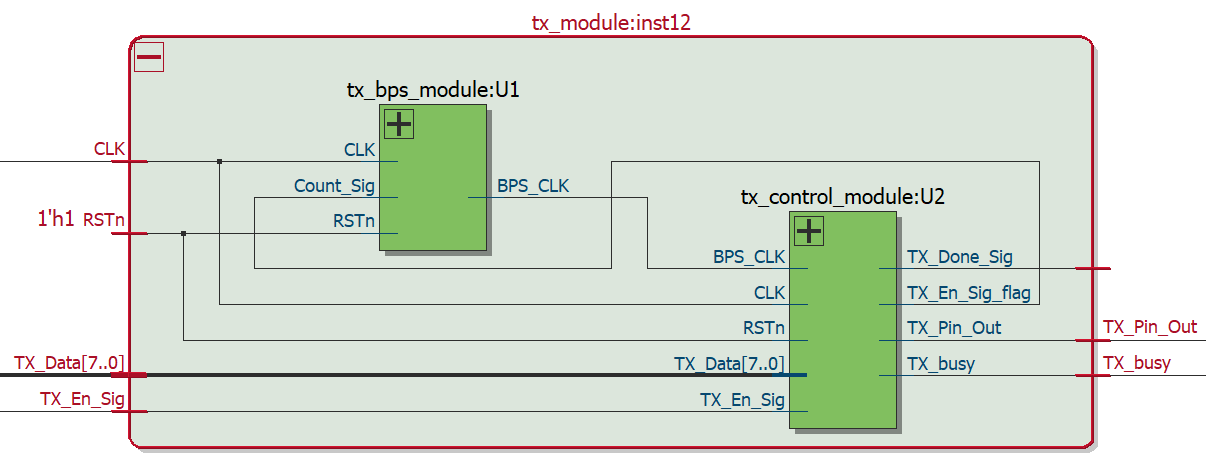
The wiring of the whole schematic diagram can be clearly seen here.
summary
With the accumulation of the previous article, the sending module is still relatively simple. If we can have a deep understanding of the receiving module, the implementation of the transmitting module is only a matter of time and details. Through the completion of these two articles, I have a further understanding of the serial port. Including the design of check bit and baud rate. The key is to have a further understanding of Verilog HDL programming language. The code is still written less, their thinking is still relatively slow, and their understanding of programming is still too shallow. I hope I can have a greater feeling next time.