RTL and integrated concept
RTL (Register Transfer Level) refers to the HDL level of the circuit by describing the logic function from register to register without paying attention to the details of register and combinational logic (such as how many logic gates are used, the connection topology between logic gates, etc.). RTL level is a higher level of abstraction than gate level. Using RTL level language to describe hardware circuits is generally much simpler and more efficient than gate level description.
- The most important feature of RTL level language is that RTL level description is a comprehensive description level.
Synthesis refers to translating design inputs such as HDL language and schematic diagram into gate level connection (net list) composed of basic logic units such as and, or and not gates, optimizing the generated logical connection according to design objectives and requirements (constraints), and outputting gate level net list files. RTL level synthesis refers to translating and optimizing RTL level source code into gate level netlist.
Basic elements and design steps of RTL level
A typical RTL design consists of the following three parts
-
Clock domain description: describes all clocks used, the master-slave and derivative relationship between clocks, and the conversion between clock domains;
-
Timing logic description (register description): describe the data transmission mode between registers according to the transformation of clock edge;
-
Combinational logic description: describe the logic combination mode and logic function of level sensitive signal.
Design steps recommended in the book:
- Function definition and module division: divide each function module according to the definition of system function and module division criteria;
- Define the interfaces of all modules: first, clearly define the interfaces of each module and complete the signal list of each module. This idea is consistent with Modular Design (Modular Design method), which is conducive to module reuse, debugging and modification;
- Design clock domain: define the derivation relationship between clocks according to the complexity of the designed clock, analyze which clock domains are in the design, and whether there is data exchange between asynchronous clock domains; For PLD device design, it is also necessary to confirm whether the global clock uses PLL/DLL to complete the functions of clock frequency division, frequency doubling and phase shift, which clocks use the global clock resource wiring and which clocks use the second global clock resource wiring; The characteristics of the global clock are: there is almost no Clock Skew, there is a certain Clock Delay, and the driving ability is the strongest; Second, the global clock is characterized by smaller Clock Shew and smaller Clock Delay, with strong clock driving ability;
- Add: Clock Jitter: refers to the temporary change of the clock cycle at a given point of the chip, so that the clock cycle may be lengthened or shortened in different cycles. Clock Skew: it is caused by different wiring length and load, resulting in inconsistent time when the same clock signal reaches two adjacent timing units. Difference: Jitter is generated inside the clock generator and is related to the internal circuit of crystal oscillator or PLL. The wiring has no effect on it. Skew is caused by different wiring lengths. The arrival delay of the rising edge of the clock of different paths is different.
- Consider the critical path of the design: the critical path refers to the path that is most difficult to meet the timing requirements in the design. The timing requirements of the design are mainly reflected in the timing indicators such as frequency, establishment time and holding time,; At the initial stage of design, the designer can roughly analyze the timing difficulties of the design (such as the highest frequency path, the lowest bit of the counter, the timing path containing complex combinational logic, etc.) according to the frequency requirements of the system, and alleviate the timing pressure of the design from the code through some timing optimization means (such as Pipeline, Retiming, logic replication, etc.), This method is more effective by relying on the automatic optimization of synthesis and wiring tools;
- Top level design: the top-down design method is recommended for RTL design, because this design method is consistent with the sequence of module planning, and is more conducive to Modular Design. It can carry out design work in parallel and improve module reuse rate;
- FSM design: FSM is one of the most important contents of logic design;
- Timing logic design: firstly, the register group is planned according to the clock domain, and then the data transmission mode between each register group is described;
- Combinational logic design: Generally speaking, large segment combinational logic is best described separately from sequential logic, which is more conducive to timing constraints and timing analysis, so as to achieve better optimization effect of synthesizer and layout and routing device.
Common RTL level modeling
Non blocking assignment, blocking assignment, continuous assignment
- For timing logic, that is, the sensitive signal list of always block is edge sensitive signal, and the non blocking assignment "< =" is used uniformly;
- For the combinational logic whose sensitive signal list of always block is level sensitive, the blocking assignment "=" is used uniformly;
- For the combinational logic described by the assign keyword, the blocking assignment "=" is used uniformly, and the variable is defined as a wire signal.
Register circuit modeling
Register and combinational logic are two basic elements of digital logic circuit. Register is generally associated with synchronous timing logic. Its characteristic is that the output can be changed only when the edge of the clock arrives.
- Register variable declaration: the register is defined as reg type, but it should be noted that the opposite is not necessarily true;
- Clock input: the data is processed on the positive or negative edge of each clock.
- Asynchronous reset / set: most register models of target devices include asynchronous reset / set terminal;
- Synchronous reset / set: any register can realize synchronous reset / set function;
- The problem of using the rising edge and falling edge of the clock at the same time: sometimes, due to the needs of data sampling or adjusting the data phase, the designer will use the posedge and nesedge of the clock in the sensitive signal list of one always, or use posedge and nesedge to operate a register circuit in the sensitive signal list of two always respectively; Under these two descriptions, when the rising edge and falling edge of the clock arrive, the register circuit will do the corresponding operation. This double edge circuit is equivalent to the single edge operation circuit using the frequency doubling clock of the original clock. This operation is not recommended; PLL/DLL and some clock circuits in the chip often have very good indicators for one edge, while the jitter, offset, slope and other indicators of the other edge are not very optimized. Sometimes using the positive and negative edges of the clock at the same time will cause some performance deterioration due to clock jitter, skew, duty cycle, slope and other problems; It is generally recommended to double the frequency of the original clock through PLL/DLL, and then use the single edge of the frequency doubling clock for operation.
Combinatorial logic modeling
The sensitive signal list of always module is the combinational logic circuit of level sensitive signal
The sensitive signal list of always module is all decision conditions and input signals. When using this structure to describe combinatorial logic, we must write the sensitive list completely. In the always block, high-level programming language can be used and blocking assignment "=" can be used. Although the signal is defined as bit reg type, the final comprehensive implementation result is not register, but combinatorial logic. Defining reg type is a pure syntax requirement.
Combinational logic circuit described by assign and other statements
This formal description of combinational logic circuit is suitable for describing those relatively simple combinational logic. Signals are generally defined as bit wire type.
Bidirectional port and three state signal modeling
All bidirectional buses shall be defined as three state signals in the top-level module, and it is prohibited to define bidirectional ports in other sub levels other than the top-level. In order to avoid inconsistency between simulation and comprehensive implementation results and facilitate maintenance, it is strongly recommended to define bidirectional bus and instantiated three state signal only at the top level, prohibit assigning high resistance state "Z" at other levels except the top level, divide bidirectional signals into input and output signals at the top level, and then transfer them to different sub modules as required, Another advantage of this is that it is easy to describe simulation incentives.
module bibus (clk, rst, sel, data_bus, addr);
input       clk, rst, sel;
input [7:0] addr;
inout [7:0] data_bus;
wire [7:0] data_in, data_out;

assign data_in = data_bus;
assign data_bus = (sel) ? data_out : 8'bZ;

decode decode_inst (.clock (clk),
                    .reset (rst),
                    .data_bus_in (data_in),
                    .addr_bus (addr),
                    .data_bus_out (data_out)
                    );
endmodule
If the enabling relationship of the three state bus is complex and not a single signal, you can use nested question mark expressions or use case statements to describe it.
- Nested question mark expressions
module complex_bibus (clk, rst, sel1, sel2, sel3, data_bus, addr);
input       clk, rst;
input       sel1, sel2, sel3;
input [7:0] addr;
inout [7:0] data_bus;

wire [7:0] data_in;
//wire [7:0] data_out; //use wire type
wire [7:0] decode_out;
wire [7:0] cnt_out;

assign data_in = data_bus;
assign data_bus = (sel1)? decode_out : ((sel2)? cnt_out : ((sel3)? 8'b11111111: 8'bZZZZZZZZ));

decode decode_inst (.clock (clk),
                    .reset (rst),
                    .data_bus_in (data_in),
                    .addr_bus (addr),
                    .data_bus_out (decode_out)
                    );

counter counter_inst (.clock (clk),
                    .reset (rst),
                    .data_bus_in (data_in),
                    .cnt_out (cnt_out)
                    );
endmodule
- Case statement (if the enabling situation is complex, it is clearer to list it through case)
input sel1, sel2, sel3;
input [7:0] addr;
inout [7:0] data_bus;

wire [7:0] data_in;
reg  [7:0] data_out; //use reg type, but not registers
wire [7:0] decode_out;
wire [7:0] cnt_out;

assign data_in = data_bus;

decode decode_inst (.clock (clk),
                    .reset (rst),
                    .data_bus_in (data_in),
                    .addr_bus (addr),
                    .data_bus_out (decode_out)
                    );

counter counter_inst (.clock (clk),
                    .reset (rst),
                    .data_bus_in (data_in),
                    .cnt_out (cnt_out)
                    );

always @ (decode_out or cnt_out or sel1 or sel2 or sel3)
    begin
       case ({sel1, sel2, sel3})
         3'b100:  data_out = decode_out;
         3'b010:  data_out = cnt_out;
         3'b001:  data_out = 8'b11111111;
         default: data_out = 8'bZZZZZZZZ;
       endcase
    end
assign data_bus = data_out;
endmodule
mux modeling
Simply use assign and?, Relatively complex conditional judgment statements such as always, if... else and case are used for modeling.
Memory modeling
Logic circuit design often uses some single port RAM, dual port RAM and ROM memory. The basic storage unit definition format in Verilog syntax is:
reg [datawidth] MemoryName [addresswidth]
For example, define a RAM8x64 with a data bit width of 8bit and an address of 63:
reg [7:0] RAM8x64 [0:63];
When using a storage unit, you cannot directly operate a bit of an address of the memory. You need to assign the storage unit to a register first, and then operate a bit of the memory.
module ram_basic (clk, CS, WR, addr, data_in, data_out, en);
input         clk;
input         CS;  //CS = 1, RAM enable
input         WR;  //WR =1 then WRite enable; WR = 0 then read enable
input         en;  //data_out enable, convert the data sequency
input  [5:0]  addr;
input  [7:0]  data_in;
output [7:0]  data_out;

 reg [7:0] RAM8x64 [0:63];
 reg [7:0] mem_data;

always @ (posedge clk)
    if (WR && CS) //WRite
        RAM8x64 [addr] <= data_in [7:0];
    else if (~WR && CS ) // read
        mem_data <= RAM8x64 [addr];

assign data_out = (en)? mem_data[7:0] : {~mem_data[7], mem_data[6:0]};
endmodule
- The RAM resources embedded in FPGA are divided into two types: Block RAM resources and distributed RAM resources. As the internal hardware resources of FPGA, BRAM will not occupy other logic resources. Distributed RAM is a RAM structure realized by look-up table and trigger.
- When using RAM and other resources, this Verilog language is usually not used for modeling. Generally, the IP core provided by the manufacturer is used to complete the relevant parameter configuration through the GUI and generate the relevant IP.
Simple clock frequency division circuit
- Even frequency division is very simple. You only need to drive a synchronous counter with a high-speed clock;
module clk_div_phase (rst, clk_200K, clk_100K, clk_50K, clk_25K);
input        clk_200K;
input        rst;
output       clk_100K, clk_50K, clk_25K;
wire         clk_100K, clk_50K, clk_25K;

reg [2:0] cnt;

always @ (posedge clk_200K or negedge rst)
   if (!rst)
      cnt <= 3'b000;
   else
      cnt <= cnt + 1;

assign clk_100K = ~cnt [0];//2 frequency division
assign clk_50K  = ~cnt [1];//4 frequency division
assign clk_25K  = ~cnt [2];//8 frequency division

endmodule
The above example completes all clock adjustments after frequency division by reversing each bit of the counter, ensuring that the phases of the three clocks after frequency division are strictly in phase and in phase with the source clock, with a common rising edge.
- Odd frequency division
module clk_3div (clk,reset,clk_out);
input clk, reset;
output clk_out;
reg[1:0] state;
reg clk1;
always @(posedge clk or negedge reset)
if(!reset)
    state<=2'b00;
else
    case(state)
        2'b00:state<=2'b01;
        2'b01:state<=2'b11;
        2'b11:state<=2'b00;
        default:state<=2'b00;
    endcase

always @(negedge clk or negedge reset)
    if(!reset)
        clk1<=1'b0;
    else
        clk1<=state[0];

assign clk_out=state[0]&clk1;
endmodule
Serial / parallel conversion modeling
According to the requirements of data sorting and quantity, shift register and RAM can be selected; For a small number of designs, shift registers can be used to complete serial / parallel conversion (serial to parallel: shift first and then output in parallel; parallel to serial: load parallel data first and then output in shift); For the serial / parallel conversion with regular arrangement order, the case statement can be used to judge and realize; For complex serial / parallel conversion, it can also be realized by state machine.
Synchronous reset and asynchronous reset
Synchronous reset
modeling
module syn_rst (clk, rst_, cnt1, cnt2);
input        clk;
input        rst_;
output [4:0] cnt1 , cnt2;
reg    [4:0] cnt1 , cnt2;

always @ (posedge clk)
   if (!rst_)
      begin
        cnt1 <= 4'b0;
        cnt2 <= 4'b0;
      end
   else
      begin
        if (cnt1 < 2'b11)
            cnt1 <= cnt1 + 1;
        else
            cnt1 <= cnt1;
        cnt2 <= cnt1 - 1;
      end
endmodule
The trigger itself of many target devices does not contain a synchronous reset port, so the synchronous reset can be realized through the following structure:
advantage
- Synchronous reset is beneficial to simulator simulation based on periodic mechanism;
- Using synchronous reset can design 100% synchronous sequential circuit, which is conducive to timing analysis, and the frequency of its comprehensive results is often higher;
- Synchronous reset only takes effect on the rising edge of the clock, which can effectively avoid metastability and errors caused by the burr of the reset circuit; When resetting and releasing the reset signal, relevant operations are carried out only when the reset level changes at the clock edge. If there are some burrs in the combined logic of the reset signal tree, the probability of collecting burrs at the clock edge is very low. Through the clock edge sampling, the combined logic burrs of the reset circuit can be filtered very effectively and the stability of the circuit can be enhanced.
shortcoming
-
The trigger itself of many target devices does not contain synchronous reset port, and the use of synchronous reset will increase a lot of logic resources;
-
The biggest problem of synchronous reset is that the effective time of the reset signal must be long enough to ensure that all triggers are effectively reset. Therefore, the duration of the synchronous reset signal must be greater than the designed maximum clock cycle to ensure that the synchronous reset signal can be sampled at the effective edge of all clocks.
-
In fact, it is not enough to only ensure that the duration of the synchronous reset signal is greater than the slowest clock cycle. The delay of the synchronous reset signal tree through all combinational logic paths and the skew caused by clock wiring should also be considered in the design. Only when the synchronous reset is greater than the maximum cycle of the clock plus the delay of the combinational logic path through which the synchronization signal passes plus the clock skew, In order to ensure reliable and complete synchronous reset.
-
In the above figure, assuming that the delay of the combinational logic of the synchronous reset logic tree is T1, the maximum delay of the reset signal propagation path is T2, the period of the slowest clock is period max, and the skew of the clock is clk2-clk1, the period of synchronous reset is Tsys_rst shall meet: Tsys_rst > Period max + (clk2-clk1) + t1 + t2;
Asynchronous reset
modeling
module asyn_rst (clk, rst_, cnt1, cnt2);
input        clk;
input        rst_;
output [4:0] cnt1 , cnt2;
reg    [4:0] cnt1 , cnt2;

always @ (posedge clk or negedge rst_)
   if (!rst_)
      begin
        cnt1 <= 4'b0;
        cnt2 <= 4'b0;
      end
   else
      begin
        if (cnt1 < 2'b11)
            cnt1 <= cnt1 + 1;
        else
            cnt1 <= cnt1;
        cnt2 <= cnt1 - 1;
      end
endmodule
advantage
- Most devices contain asynchronous reset ports, which will save logic resources;
- Asynchronous reset design is simple;
- Most FPGA s have dedicated global set reset resources (GSR). Using GSR resources, asynchronous reset can minimize the skew of all registers.
shortcoming
- The function and release of asynchronous reset are not directly related to the clock edge, and the problem is not obvious when the asynchronous reset works. However, when the asynchronous reset is released, if the release time of asynchronous reset is almost the same as the arrival time of the effective edge of the clock, it is easy to cause the metastable output of the trigger and logic error;
- If the combinational logic of the asynchronous reset logic tree produces a burr, the effective edge of the burr will cause the trigger to be reset by mistake, resulting in logic error.
Recommended reset circuit design - asynchronous reset, synchronous release
- The recommended reset circuit design method is asynchronous reset and synchronous release, which can effectively inherit the advantages of simple asynchronous reset design and overcome the risks and defects of asynchronous reset; Compared with pure asynchronous reset, it reduces the possibility of metastable state caused by asynchronous reset signal release. Compared with synchronous reset, it can identify the reset signal that cannot be detected in synchronous reset.
- Using asynchronous reset and synchronous release in FPGA can save device resources and obtain stable and reliable reset effect.
- Asynchronous reset and synchronous release can not only detect the reset signal quickly and do not need to be reset for more than one clock cycle, but also solve the metastable problem during release (reduce the probability of metastable occurrence).
module asyn_rst_syn_release(clk, rst_, cnt1, cnt2);

input        clk;
input        rst_;
output [4:0] cnt1 , cnt2;
reg    [4:0] cnt1 , cnt2;
// reset release circuit
reg reset_reg;

always @ (posedge clk)
     reset_reg <= rst_;    //Asynchronous reset synchronization

always @ (posedge clk or negedge reset_reg)
   if (!reset_reg)
      begin
        cnt1 <= 4'b0;
        cnt2 <= 4'b0;
      end
   else
      begin
        if (cnt1 < 2'b11)
            cnt1 <= cnt1 + 1;
        else
            cnt1 <= cnt1;
        cnt2 <= cnt1 - 1;
      end

endmodule
- There are many specific design methods for asynchronous reset and synchronous release. The key is how to ensure the synchronous release of the reset signal. The method of this example is to sample the system clock when the reset signal is released, and then send the reset signal to the asynchronous reset end of the register.
- The so-called "asynchronous reset" refers to the reset port of D trigger. It is asynchronous, but the asynchronous reset signal has been synchronized in the design, so the author (Crazybingo) believes that this is only "asynchronous reset" in a sense.
- The so-called "synchronous release" is actually because we have designed the synchronous logic circuit. The external reset signal will not compete with the clk signal when the release occurs, and the whole system will be synchronized with the global clock clk signal.
- Another advantage of the design method of using the clock to register the externally input asynchronous reset signal for a beat and then send it to the trigger asynchronous reset port is that when doing STA (static timing analysis), the timing tool will automatically check the relationship between the asynchronous reset signal after synchronization and the arrival / Removal time of the clock, If the arrival / cancellation time cannot be met due to the skew caused by wiring, STA tool will report the path to help the designer further analyze the problem.
module system_ctrl     //Asynchronous reset, synchronous release
//==================< port >==================================================
(
//globel clock ----------------------------------
input  wire                 clk                 , //Clock, 50Mhz
input  wire                 rst_n               , //Reset, low level active
//user interface --------------------------------
input  wire                 a                   , //Input signal
output reg                  b                     //output signal
);

//==========================================================================
//==Synchronization design of asynchronous reset
//==========================================================================
reg        sys_rst_n_r;
reg        sys_rst_n;

always @(posedge clk or negedge rst_n)
begin
    if(!rst_n) begin
        sys_rst_n_r <= 1'b0;
        sys_rst_n   <= 1'b0;
    end
    else begin
        sys_rst_n_r <= 1'b1;
        sys_rst_n   <= sys_rst_n_r; //Notice the rst here_ sync_ N is the reset signal we really output to the system
    end
end

always @(posedge clk or negedge sys_rst_n)   //Note that the signal after synchronization is still processed as asynchronous reset signal, which is recommended by Altera
begin
    if(!sys_rst_n)
        b <= 0;
    else
        b <= a;
end

endmodule
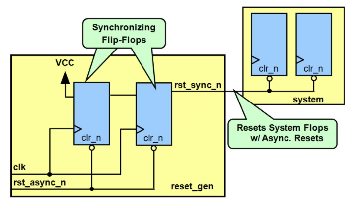
The figure above is the schematic diagram of asynchronous reset and synchronous release recommended by Altera
module reset_gen ( output rst_sync_n, input clk, rst_async_n);  //This module corresponds to the logic in the previous yellow box, and the output signal is still processed as asynchronous reset signal in the later circuit
reg rst_s1, rst_s2;
wire rst_sync_n ;

always @ (posedge clk, posedge rst_async_n)
    if (rst_async_n)
         begin
            rst_s1 <= 1'b0;
            rst_s2 <= 1'b0;
        end
    else
        begin
            rst_s1 <= 1'b1;		//For Altera FPGA
            rst_s2 <= rst_s1;
        end

assign rst_sync_n = rst_s2; //Notice the rst here_ sync_ N is the reset signal we really output to the system

endmodule
Xilinx
Xilinx's FPGA supports high-level reset, and its FILP flop also supports synchronous / asynchronous reset. Reset criteria:
- Minimize the use of reset, especially the use of global reset. Do not use reset if you can. - use local reset if you must use reset;
- If it is necessary to reset, try to use synchronous reset on synchronous and asynchronous reset, - where asynchronous reset is necessary,
Adopt "asynchronous reset and synchronous release"; - Reset level: select high level reset;
For the same trigger logic, because asynchronous and synchronous reset are supported at the same time, asynchronous reset will not save resources; For other resources, such as DSP48, synchronous reset saves more resources.
First, for DSP48, there are also some registers inside (only synchronous reset is supported). If asynchronous reset is used, the registers with asynchronous reset in the external Slice will be used additionally. When synchronous reset is used, the registers inside DSP48 can be used; Xilinx FPGA, for DSP48 and BRAM resources, using synchronous reset saves resources more than asynchronous reset.
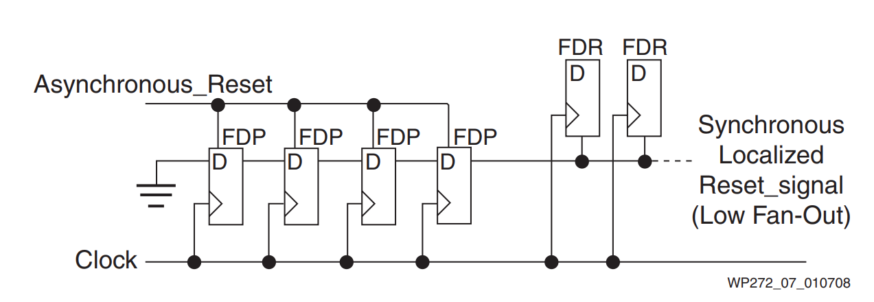
For high-level reset, if asynchronous reset and synchronous release are used, the D input of the first register is 0. Here, four triggers are used to beat synchronization.
always @(posedge clk or posedge rst_async)
begin
    if(rst_async == 1'b1) begin
        rst_sync_reg1 <= 1'b1;	//FPGA high level reset of Xilinx
        rst_sync_reg2 <= 1'b1;
        rst_sync_reg3 <= 1'b1;
        rst_sync_reg4 <= 1'b1;
    end
    else begin
        rst_sync_reg1 <= 1'b0;
        rst_sync_reg2 <= rst_sync_reg1;
        rst_sync_reg3 <= rst_sync_reg2;
        rst_sync_reg4 <= rst_sync_reg3;
    end
end

wire sys_rst;
assign sys_rst = rst_sync_reg4;

always @(posedge clk)    //The signal after synchronization is treated as a synchronous reset signal
begin
    if(sys_rst == 1'b1) begin
        data_out_rst_async <= 1'b0;
    end
    else begin
        data_out_rst_async <= a & b & c & d;
    end
end
If the signal after synchronization is processed as a synchronization reset signal:
rst_ Once async asynchronous reset is given, the four registers RST for synchronization_ sync_ Reg1 ~ 4 immediately outputs high level "1", detects synchronous reset at the rising edge of the next clock and outputs data_out_rst_async reset;
After the asynchronous reset signal is released, it passes through synchronous sys_rst is released synchronously at the edge of the clock after a certain period;
If the signal after synchronization is processed as asynchronous reset signal:
The difference lies in the asynchronous reset signal rst_ Once async is generated, the output will be reset immediately and released synchronously. It seems that this kind of processing is more in line with asynchronous reset and synchronous release.
So why does Xilinx white paper still use sys_ What does RST do according to synchronous reset? Considering comprehensively, there may be such factors:
-
The difference between synchronous reset and synchronous reset is that the reset time is a little later. It should be detected at the next edge of the clock, but the input RST can still be recognized_ Async asynchronous reset signal, so from the perspective of reset, it can achieve the effect of reset after;
-
According to Xilinx reset criteria, we know that synchronous reset has many advantages over asynchronous reset. For details, see: Xilinx FPGA reset strategy white paper (WP272) , since there is no functional difference between the two for subsequent reset, synchronous reset is preferred;
Altera
Altera's FPGA has low-level reset, and its trigger has only asynchronous reset port. Therefore, if you want to use synchronous reset, you need additional resources to realize it. This is also the reason for the saying that "asynchronous reset saves resources".
See the above for specific circuit and code
Modeling with case and if... else
slightly
Integrable Verilog grammar subset
In RTL modeling, the use of comprehensive Verilog syntax is a very small subset of the whole Verilog syntax. In fact, the common keywords that can be integrated in Verilog are very limited, which just reflects the essence of Verilog language as a hardware description language. As HDL, the essence of Verilog is to convert the circuit into a language form smoothly and reasonably, and using fewer keywords can effectively convert the circuit into a comprehensive RTL language structure.
Examples of common RTL syntax structures:
- module declaration: module... endmodule;
- Port declaration: input, outpu t, inout;
- Signal type: wire, reg, tri, etc. integer is usually used for index in for statement;
- Parameter definition: parameter
- Operation operators: logical operation, shift operation and arithmetic operation;
- Comparative judgment: case... endcase (casex/casez), if... else;
- Continuous assignment: assign, question mark expression
- always module: modeling timing and combinatorial logic
- Syntax separator: begin... end
- Task definition: task... endtask
- Circular statement: for
Design example of CPU read / write PLD register interface
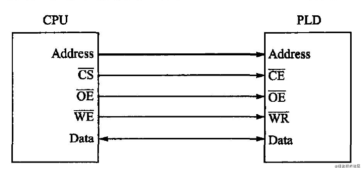
- CS: film selection (low effective, input)
- OE: output enable signal (low effective, input)
- WR: read / write indication, low read data, high write data (input)
- Address: address bus (input)
- Data: bidirectional data bus (inout)
Address decoder circuit
module decode (CS_, OE_, WR_, Addr, my_wr, my_rd, CS_reg1, CS_reg2, CS_reg3);

input        CS_, OE_, WR_;
input  [7:0] Addr;

output       my_wr, my_rd;
output       CS_reg1, CS_reg2, CS_reg3;

reg          CS_reg1, CS_reg2, CS_reg3;

assign my_wr = (!WR_) && (!CS_) && (!OE_);
assign my_rd = (WR_)  && (!CS_) && (!OE_);

always @ (Addr or CS_)
  if (!CS_)
     begin
       case (Addr)
          8'b 11110000: CS_reg1 <= 1'b1;
          8'b 00001111: CS_reg2 <= 1'b1;
          8'b 10100010: CS_reg3 <= 1'b1;
          default:     begin
                           CS_reg1 <= 1'b0;
                           CS_reg2 <= 1'b0;
                           CS_reg3 <= 1'b0;
                       end
       endcase
     end


endmodule
Read register
module read_reg (clk, rst, data_out,  my_rd, CS_reg1, CS_reg2, CS_reg3, reg1, reg2, reg3);

input        clk, rst, my_rd, CS_reg1, CS_reg2, CS_reg3;
input  [7:0] reg1, reg2, reg3;
output [7:0] data_out;
reg    [7:0] data_out;

  always @ (posedge clk or negedge rst)
      if (!rst)
         data_out <= 8'b0;
      else
         begin
            if (my_rd)
                begin
                     if (CS_reg1)
                         data_out <= reg1;
                     else if (CS_reg2)
                         data_out <= reg2;
                     else if (CS_reg3)
                         data_out <= reg3;
                end
            else
                data_out <= 8'b0;

         end

endmodule
Write register
module write_reg (clk, rst, data_in,  my_wr, CS_reg1, CS_reg2, CS_reg3, reg1, reg2, reg3);

input        clk, rst, my_wr, CS_reg1, CS_reg2, CS_reg3;
input  [7:0] data_in;
output [7:0] reg1, reg2, reg3;
reg    [7:0] reg1, reg2, reg3;

  always @ (posedge clk or negedge rst)
      if (!rst)
         begin
              reg1 <= 8'b0;
              reg2 <= 8'b0;
              reg3 <= 8'b0;
         end
      else
         begin
            if (my_wr)
                begin
                     if (CS_reg1)
                         reg1 <= data_in;
                     else if (CS_reg2)
                         reg2 <= data_in;
                     else if (CS_reg3)
                         reg3 <= data_in;
                end
            else
                begin
                     reg1 <= reg1;
                     reg2 <= reg2;
                     reg3 <= reg3;
                end

         end

endmodule
top floor
module top (clk_cpu, rst, CS_, OE_, WR_, Addr, data_bus);

input   clk_cpu, rst;
input   CS_, OE_, WR_;
input [7:0] Addr;
inout [7:0] data_bus;

wire [7:0] data_in;
wire [7:0] data_out;
wire       my_wr, my_rd;
wire       CS_reg1, CS_reg2, CS_reg3; // the register selection
wire [7:0] reg1, reg2, reg3;          // the register to be read and written


assign data_in = data_bus;
assign data_bus = ((!CS_) && (!OE_))? data_out : 8'bZZZZZZZZ;

decode decode_u1  (.CS_(CS_),
                   .OE_(OE_),
                   .WR_(WR_),
                   .Addr(Addr),
                   .my_wr(my_wr),
                   .my_rd(my_rd),
                   .CS_reg1(CS_reg1),
                   .CS_reg2(CS_reg2),
                   .CS_reg3(CS_reg3)
                   );

write_reg write_reg_u1 ( .clk(clk_cpu),
                         .rst(rst),
                         .data_in(data_in),
                         .my_wr(my_wr),
                         .CS_reg1(CS_reg1),
                         .CS_reg2(CS_reg2),
                         .CS_reg3(CS_reg3),
                         .reg1(reg1),
                         .reg2(reg2),
                         .reg3(reg3)
                         );

read_reg read_reg_u1  ( .clk(clk_cpu),
                         .rst(rst),
                         .data_out(data_out),
                         .my_rd(my_rd),
                         .CS_reg1(CS_reg1),
                         .CS_reg2(CS_reg2),
                         .CS_reg3(CS_reg3),
                         .reg1(reg1),
                         .reg2(reg2),
                         .reg3(reg3)
                         );

endmodule
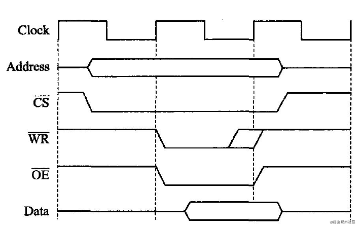
Use OE/WR edge to read and write
The description of edge reading and writing registers using OE or WR seems simpler than the description of synchronous reading and writing registers using CPU clock introduced earlier, but readers must be clear that there are two preconditions for this method to work normally:
- The rising edge of OE can effectively sample the data bus, that is, when the rising edge of OE samples the data bus, both Setup and Hold can be guaranteed to meet;
- Both WR and CS signals are wider than OE signals, that is, when OE rising edge reads and writes registers, CS and WR signals always remain valid.
Only when these two conditions are met at the same time can we ensure that the edge reading and writing PLD register circuit using OE is reliable.
/******************************************/
module decode (CS_, WR_, Addr, my_wr, my_rd, CS_reg1, CS_reg2, CS_reg3);

input        CS_, WR_;
input  [7:0] Addr;

output       my_wr, my_rd;
output       CS_reg1, CS_reg2, CS_reg3;

reg          CS_reg1, CS_reg2, CS_reg3;

assign my_wr = (!WR_) && (!CS_);
assign my_rd = (WR_)  && (!CS_);

always @ (Addr or CS_)
  if (!CS_)
     begin
       case (Addr)
          8'b 11110000: CS_reg1 <= 1'b1;
          8'b 00001111: CS_reg2 <= 1'b1;
          8'b 10100010: CS_reg3 <= 1'b1;
          default:     begin
                           CS_reg1 <= 1'b0;
                           CS_reg2 <= 1'b0;
                           CS_reg3 <= 1'b0;
                       end
       endcase
     end
endmodule
/******************************************/
module read_reg (OE_, rst, data_out,  my_rd, CS_reg1, CS_reg2, CS_reg3, reg1, reg2, reg3);

input        OE_, rst, my_rd, CS_reg1, CS_reg2, CS_reg3;
input  [7:0] reg1, reg2, reg3;
output [7:0] data_out;
reg    [7:0] data_out;

  always @ (posedge OE_ or negedge rst)
      if (!rst)
         data_out <= 8'b0;
      else
         begin
            if (my_rd)
                begin
                     if (CS_reg1)
                         data_out <= reg1;
                     else if (CS_reg2)
                         data_out <= reg2;
                     else if (CS_reg3)
                         data_out <= reg3;
                end
            else
                data_out <= 8'b0;

         end
endmodule
/******************************************/
module write_reg (OE_, rst, data_in,  my_wr, CS_reg1, CS_reg2, CS_reg3, reg1, reg2, reg3);

input        OE_, rst, my_wr, CS_reg1, CS_reg2, CS_reg3;
input  [7:0] data_in;
output [7:0] reg1, reg2, reg3;
reg    [7:0] reg1, reg2, reg3;

  always @ (posedge OE_ or negedge rst)
      if (!rst)
         begin
              reg1 <= 8'b0;
              reg2 <= 8'b0;
              reg3 <= 8'b0;
         end
      else
         begin
            if (my_wr)
                begin
                     if (CS_reg1)
                         reg1 <= data_in;
                     else if (CS_reg2)
                         reg2 <= data_in;
                     else if (CS_reg3)
                         reg3 <= data_in;
                end
            else
                begin
                     reg1 <= reg1;
                     reg2 <= reg2;
                     reg3 <= reg3;
                end

         end

endmodule
/******************************************/
module top (rst, CS_, OE_, WR_, Addr, data_bus);

input       rst;
input        CS_, OE_, WR_;
input [7:0] Addr;
inout [7:0] data_bus;

wire [7:0] data_in;
wire [7:0] data_out;
wire       my_wr, my_rd;
wire       CS_reg1, CS_reg2, CS_reg3; // the register selection
wire [7:0] reg1, reg2, reg3;          // the register to be read and written

assign data_in = data_bus;
assign data_bus = ((!CS_) && (!OE_))? data_out : 8'bZZZZZZZZ;

decode decode_u1  (.CS_(CS_),
                 //  .OE_(OE_),
                   .WR_(WR_),
                   .Addr(Addr),
                   .my_wr(my_wr),
                   .my_rd(my_rd),
                   .CS_reg1(CS_reg1),
                   .CS_reg2(CS_reg2),
                   .CS_reg3(CS_reg3)
                   );

write_reg write_reg_u1 ( .OE_(OE_),
                         .rst(rst),
                         .data_in(data_in),
                         .my_wr(my_wr),
                         .CS_reg1(CS_reg1),
                         .CS_reg2(CS_reg2),
                         .CS_reg3(CS_reg3),
                         .reg1(reg1),
                         .reg2(reg2),
                         .reg3(reg3)
                         );

read_reg read_reg_u1  (  .OE_(OE_),
                         .rst(rst),
                         .data_out(data_out),
                         .my_rd(my_rd),
                         .CS_reg1(CS_reg1),
                         .CS_reg2(CS_reg2),
                         .CS_reg3(CS_reg3),
                         .reg1(reg1),
                         .reg2(reg2),
                         .reg3(reg3)
                         );

endmodule
/******************************************/
If the decoding circuit is combinational logic, the decoding result may have burrs. In addition, the timing of CPU bus may be damaged under the change of voltage, temperature and environment, resulting in the deterioration of the timing margin of OE, WR, CS and other signals. If the level of the decoding result is used as a level sensitive always module at this time, Reading and writing registers (such as read_reg.v and write_reg.v in the Example-4-21\ asyn_bad directory) will cause reading and writing errors due to burrs and error levels. Therefore, the level of OE or WR is used as a sensitive signal for reading and writing.