Device: Xilinx zynq 7035
Version: vivado2019.2
Implementation: 10.1376G serdes, a 6664B coded 4-Pair serdes routine with 64bit input and 64bit output, and the reference clock is 153.6MHz
Objective: to record the process from simulation to on-board debugging for easy recall
Detailed settings of IP core
First tab GT Selection


Second tab GT Line Rate,RefClk Selection


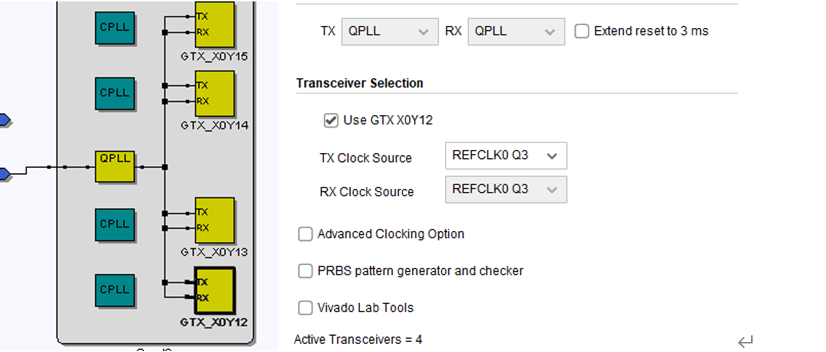
Set the clock pin position and serdes pin position. (how to set the position of GTX according to the pins given by the hardware engineer? Supplement at the end)
The third tab is Encoding and Clocking
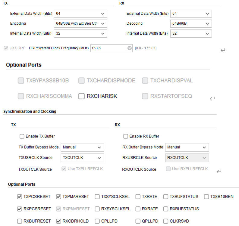
The fourth tab is Comma Alignment and Equalization
Comma Alignment does not need to be set
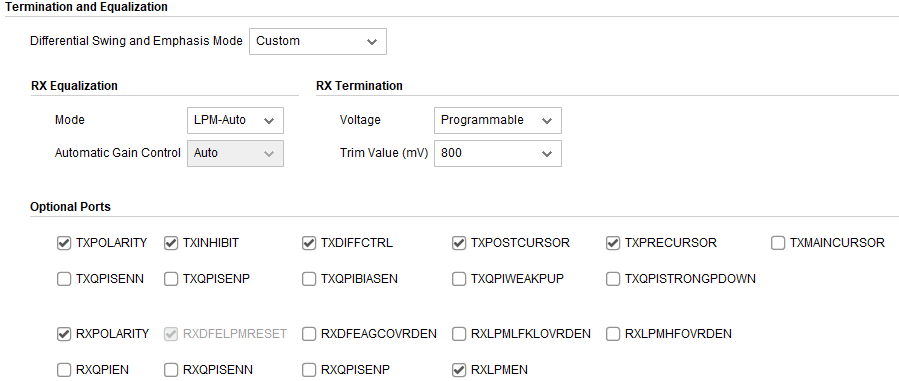
Fifth tab PCIe, SATA, PRBS
Most do not choose
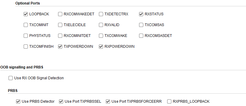
The sixth and seventh tabs have no to select.
Final Summary
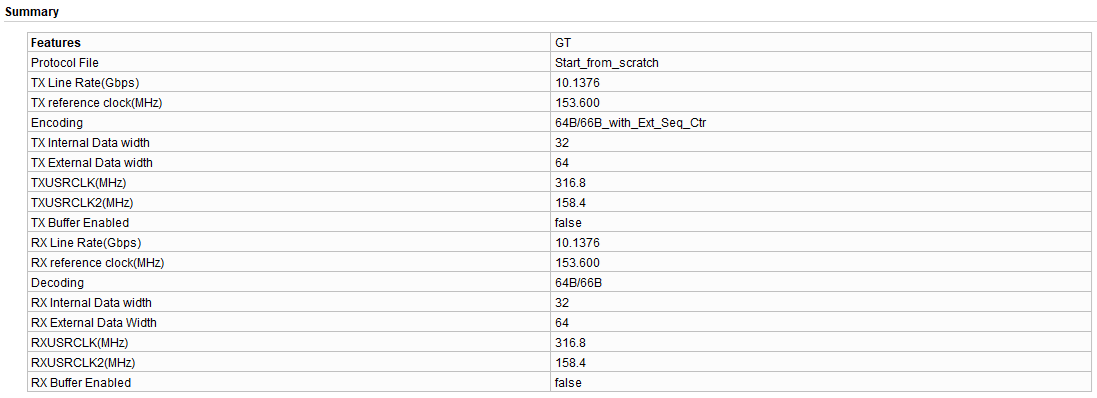
Finally, after generating the IP core, right-click the IP core and click open IP example design to generate an example project
Use of IP example
Because this IPexample has its own data sending and data verification module, in practical application, we need to lead out the data interface to be sent and the interface to be received, and we need to modify this example.
The key change points are described here:
gtwizard_ 0_ In exdes. V
(1) Input / output interface
DRP_CLK is generally single ended input, which needs to be changed here
TRACK_DATA_OUT this is not required
Add serdes transceiver reset interface
An interface for receiving and transmitting data is added. Each channel of sending and receiving includes sending and receiving data, random clock and reset
Add loopback configuration interface
(2)gtwizard_0_support module, modify the following contents to export the input / output data interface to the top-level port
.gt0_data_valid_in              (1'b1),
.gt1_data_valid_in              (1'b1),
.gt2_data_valid_in              (1'b1),
.gt3_data_valid_in              (1'b1),

.gt0_loopback_in                (i_loopback[2:0]),
.gt1_loopback_in                (i_loopback[5:3]),
.gt2_loopback_in                (i_loopback[8:6]),
.gt3_loopback_in                (i_loopback[11:9]),

.gt0_rxdata_out
.gt0_txdata_in . . . . . . . . . . . . . . . . . .
All these need to be changed slightly. There is no space to list all of them here. It is easy to see them directly through the comparison software
(3) Lead the input and output follow-up clock and reset to the top-level port
(4) Note whether the initial value of scrambling code is consistent with the opposite end
In addition to the above, the routine also has a big pit to avoid. (dry goods)
gtwizard_0_GT_USRCLK_SOURCE.v file
add to
       gtwizard_0_CLOCK_MODULE #
    (
        .MULT                           (2.0),
        .DIVIDE                         (1),
        .CLK_PERIOD                     (3.156),
        .OUT0_DIVIDE                    (4.0),
        .OUT1_DIVIDE                    (2),
        .OUT2_DIVIDE                    (1),
        .OUT3_DIVIDE                    (1)
    )
    rxoutclk_mmcm1_i0
    (
        .CLK0_OUT                       (GT0_RXUSRCLK2_OUT),
        .CLK1_OUT                       (GT0_RXUSRCLK_OUT),
        .CLK2_OUT                       (),
        .CLK3_OUT                       (),
        .CLK_IN                         (gt0_rxoutclk_i),
        .MMCM_LOCKED_OUT                (GT0_RXCLK_LOCK_OUT),
        .MMCM_RESET_IN                  (GT0_RX_MMCM_RESET_IN)
    );

    gtwizard_0_CLOCK_MODULE #
    (
        .MULT                           (2.0),
        .DIVIDE                         (1),
        .CLK_PERIOD                     (3.156),
        .OUT0_DIVIDE                    (4.0),
        .OUT1_DIVIDE                    (2),
        .OUT2_DIVIDE                    (1),
        .OUT3_DIVIDE                    (1)
    )
    rxoutclk_mmcm1_i1
    (
        .CLK0_OUT                       (GT1_RXUSRCLK2_OUT),
        .CLK1_OUT                       (GT1_RXUSRCLK_OUT),
        .CLK2_OUT                       (),
        .CLK3_OUT                       (),
        .CLK_IN                         (gt1_rxoutclk_i),
        .MMCM_LOCKED_OUT                (GT1_RXCLK_LOCK_OUT),
        .MMCM_RESET_IN                  (GT1_RX_MMCM_RESET_IN)
    );

    gtwizard_0_CLOCK_MODULE #
    (
        .MULT                           (2.0),
        .DIVIDE                         (1),
        .CLK_PERIOD                     (3.156),
        .OUT0_DIVIDE                    (4.0),
        .OUT1_DIVIDE                    (2),
        .OUT2_DIVIDE                    (1),
        .OUT3_DIVIDE                    (1)
    )
    rxoutclk_mmcm1_i2
    (
        .CLK0_OUT                       (GT2_RXUSRCLK2_OUT),
        .CLK1_OUT                       (GT2_RXUSRCLK_OUT),
        .CLK2_OUT                       (),
        .CLK3_OUT                       (),
        .CLK_IN                         (gt2_rxoutclk_i),
        .MMCM_LOCKED_OUT                (GT2_RXCLK_LOCK_OUT),
        .MMCM_RESET_IN                  (GT2_RX_MMCM_RESET_IN)
    );


    gtwizard_0_CLOCK_MODULE #
    (
        .MULT                           (2.0),
        .DIVIDE                         (1),
        .CLK_PERIOD                     (3.156),
        .OUT0_DIVIDE                    (4.0),
        .OUT1_DIVIDE                    (2),
        .OUT2_DIVIDE                    (1),
        .OUT3_DIVIDE                    (1)
    )
    rxoutclk_mmcm1_i3
    (
        .CLK0_OUT                       (GT3_RXUSRCLK2_OUT),
        .CLK1_OUT                       (GT3_RXUSRCLK_OUT),
        .CLK2_OUT                       (),
        .CLK3_OUT                       (),
        .CLK_IN                         (gt3_rxoutclk_i),
        .MMCM_LOCKED_OUT                (GT3_RXCLK_LOCK_OUT),
        .MMCM_RESET_IN                  (GT3_RX_MMCM_RESET_IN)
);
The modification here is particularly important. It feels like a BUG in xilinx. If it is not changed here, there will be no problem with the simulation. However, when debugging on the board, as long as the serdes0 interface is not connected, other interfaces will be unstable. The reason can be understood through code
Finally, the top layer is exemplified as:
   gtwizard_0_exdes
gtwizard_0_exdes_i
(
         .Q3_CLK0_GTREFCLK_PAD_N_IN           (tx_refclk_n_r),
         .Q3_CLK0_GTREFCLK_PAD_P_IN           (tx_refclk_p_r),
    .DRP_CLK_IN                          (drp_clk_r),
        .RXN_IN                              (rxn_in_i),
        .RXP_IN                              (rxp_in_i),
        .TXN_OUT                             (txn_out_i),
        .TXP_OUT                             (txp_out_i),
    .o_gtwiz_userclk_rx_usrclk2_int ( w_gtwiz_userclk_rx_usrclk2_int ),
    .o_gtwiz_userclk_tx_usrclk2_int ( w_gtwiz_userclk_tx_usrclk2_int ),

    .o_gt_rxfsmresetdone           ( w_gt_rxfsmresetdone           ),
    .o_gt_txfsmresetdone           ( w_gt_txfsmresetdone           ),
    .o_rx_header                    ( w_rx_header                   ),
    .o_rx_valid                     ( w_rx_valid                    ),
    .o_rx_data                      ( w_rx_data                     ),

    .i_tx_header                    ( w_tx_header                   ),
    .i_tx_valid                     ( w_tx_valid                    ),
    .i_tx_sequence                  ( w_tx_sequence                 ),
    .i_tx_data                      ( w_tx_data                     ),

    .i_soft_reset                   (0             ),
    .i_loopback                     (0           )
);
Take the first serdes as an example
w_gtwiz_userclk_tx_usrclk2_int[0] is the first serdes transmission clock, and the clock is 158.4M
w_ tx_ Cycle count with sequence0 fixed to 0-32
w_tx_valid0, when w_ tx_ W when sequence0 = 32_ tx_ Valid0 = 0, indicating the current input w_tx_data0 is invalid, valid at other times, and w_tx_valid0 = 1.
Reception is similar
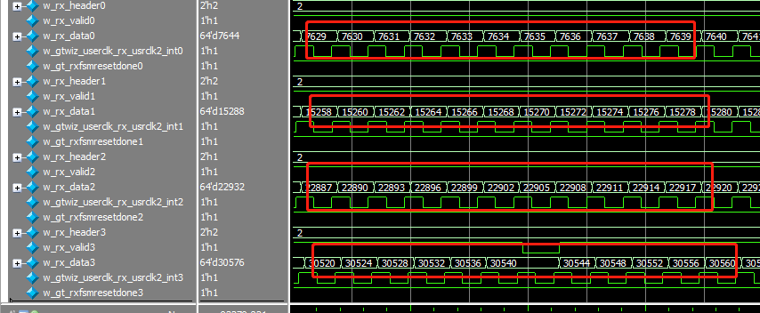
Input an addend and connect the sedes output pin directly to the input pin (during simulation) to see whether the received data is also an addend.
The project can be directly used for on-board debugging. Optical port 1 and optical port 2 are directly used for optical fiber docking. If the received data is captured through ILA, it is normal.
After adding pin and clock constraints, the project can be directly used in practical applications.
enclosure
Download address:
SERDES_ In 10g.rar
gtwizard_0_ex_yuanshi is a project directly generated for IP example,
gtwizard_0_ex_xiugai is the project modified on the above basis.
In the gtwizard_ 0_ ex_ Find ah tb.tcl in the xiugai folder. After modifying the file path in TCL, you can directly run modelsim (modelsim should configure the library file in advance)
The running result is shown in the figure below, i.e. successful
Written on October 16, 2021
For communication, QQ: 172146579