1. What is SPI protocol
SPI (Serial Peripheral Interface) communication protocol is a synchronous serial interface technology proposed by Motorola Company. It is a high-speed, full-duplex, synchronous communication bus. Only four pins are used to control and transmit data in the chip. It is widely used in EEPROM, Flash, RTC (real-time clock), ADC (digital-to-analog converter), DSP (Digital signal processor) and digital signal decoder are one of the common and important low-speed communication protocols.
The advantage of SPI protocol is that it supports full-duplex communication, and the communication mode is simple, and the relative data transmission rate is fast. The disadvantage is that there is no specified flow control, no response mechanism, and there is some deficiency in data reliability.
2. SPI Agreement Details
2.1, SPI Protocol Physical Layer
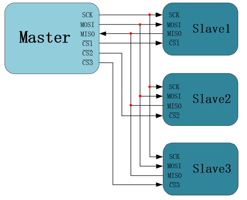
The communication mode of SPI communication device is master-slave communication mode. There are master-slave communication modes for both sides of communication, depending on the slave device. Number of connections between SPI communication devices can be divided into one master slave and one master slave.
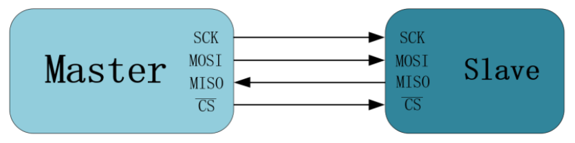
SPI bus transmission can be accomplished with only four wires, each of which serves the following purposes:
- SCK (Serial Clock): A clock signal line used to synchronize communication data. Generated by the communication host, determines the rate of communication. Different devices support different maximum clock frequencies.
- MOSI (Master Output, Slave Input): Primary device output/Primary device input pin. Host data is output from this signal line, and read from the host to the data sent from the host in the direction from the host to the slave.
- MISO (Master Input, Slave Output): Primary device input/output pin. Host reads data from this signal line, from this signal line to host, and the data direction is from machine to host.
- CS (Chip Select): Selection signal line. When more than one SPI is connected from the device to the SPI host, the other signal lines SCK, MOSI and MISO of the device are simultaneously connected to the same SPI bus, that is, they are used together regardless of how many slave devices there are. Each slave device has its own chip selection signal line, that is, how many slave devices there are and how many chip selection signal lines there are. In a communication system consisting of SPI, the slave device of communication is determined by CS chip selection signal. Low level valid during communication, indicating corresponding slave is selected
2.2, SPI protocol layer
2.2.1, CPOL/CPHA and communication modes
There are four modes for SPI bus transmission, which are defined by clock polarity (CPOL, Clock Polarity) and clock phase (CPHA, Clock Phase). The CPOL parameter specifies the level of idle state of SCK clock signal, and the CPHA specifies whether the data is sampled along the rise or decrease of the SCK clock.
Polarity of SPI Bus--Clock Polarity
Clock polarity determines whether the clock signal is high or low when the SPI bus is idle. CPOL = 1: indicates a high level when idle; CPOL = 0: indicates a low level when idle.
Phase of SPI Bus--Clock Phase
The clock phase determines which jump along the SPI bus begins to sample data. CPHA = 0: Sampling along the first hop of the clock signal SCK; CPHA = 1: Sample along the second hop of the clock signal SCK.
The time series of these four modes are shown in the following figure:
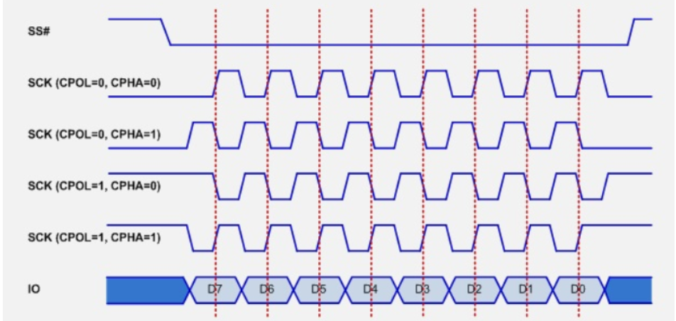
- Mode 0: CPOL= 0, CPHA=0. The SCK serial clock line is idle for low level, data is sampled at the rising edge of the SCK clock, and data is switched at the decreasing edge of the SCK clock.
- Mode 1: CPOL= 0, CPHA=1. The SCK serial clock line is idle for low level, data is sampled at the descending edge of the SCK clock, and data is switched at the rising edge of the SCK clock.
- Mode 2: CPOL= 1, CPHA=0. The SCK serial clock line is idle for high level, data is sampled along the descending edge of the SCK clock, and data is switched along the rising edge of the SCK clock
- Mode 3: CPOL= 1, CPHA=1. The SCK serial clock line is idle for high level, data is sampled at the rising edge of the SCK clock, and data is switched at the decreasing edge of the SCK clock.
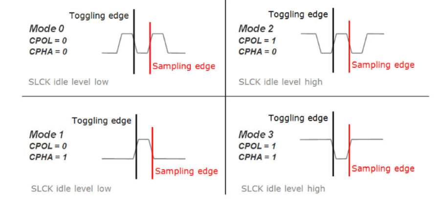
Mode 0 and mode 3 are often used (after all, few data are collected along the downward edge). The following figure describes the relationship between the data switching (Toggling) locations and the data sampling locations for the four mode data lines MOSI and MIO.
2.3, SPI protocol communication process
The following is an example of mode 0 to illustrate the basic communication process of SPI:
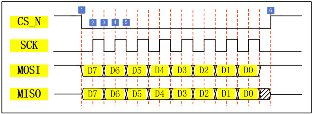
SCK, MOSI, CS_N signals are generated by host control, SCK is clock signal to synchronize data, MOSI is host output slave input signal, host transmits data to slave through this signal line, CS_N is the chip selection signal used to select slave equipment, low level is valid; The signal of the MISO is generated by the slave, through which the host reads the slave data. The signals of MOSI and MISO are only in CS_N is only valid at low levels and transmits one bit of data at each clock cycle of SKK, MOSI and MIO.
At icon 1 in the diagram, CS_ The N signal line changes from high to low, which is the starting signal for SPI communication. CS_N is the exclusive signal line for each slave when the slave is in its own CS_ When the N-line detects the start signal, it knows that it is selected by the host and starts preparing to communicate with the host. At symbol 6 in the diagram, CS_ The N signal changes from low to high, which is the stop signal of SPI communication. It indicates the end of this communication and is cancelled from the selected state of the computer.
SPI uses MOSI and MISO signal lines to transmit data and SCK signal lines to synchronize data. The MOSI and MISO data lines transmit one bit of data in each clock cycle of the SKK, and the data input and output occur simultaneously. MSB-first or LSB-first is not mandatory for data transmission, but MSB-first mode is generally used to ensure the same protocol is used between two SPI communication devices. The output of MOSI and MISO data varies during the decline of the SK and is sampled during the rise of the SK. That is, at the rising time of SCK, the data of MOSI and MISO are valid, high level means data "1" and low level means data "0". At other times, the data is invalid, and MOSI and MISO prepare for the next representation.
SPI can transfer data 8 or 16 bits per time, and there is no limit on the number of units per transmission.
2.4. Characteristics of SPI protocol
- The SPI protocol is a master-slave architecture that differentiates slaves (addressing methods) by the chip selection signal CS.
- The SPI protocol is a Synchronous transmission protocol in which both sides of the communication use the clock signal SCK generated by the host as the reference signal for data exchange.
- SPI protocol is a full duplex serial communication protocol, in which both master and slave can exchange data.
- SPI protocol has 4 communication modes and communicates according to the agreed mode between the two parties
2.5. Advantages and disadvantages of SPI protocol
Advantages:
- Full Duplex Serial Communication
- Simple hardware architecture
- High-speed data transfer rate (compared to UART, IIC)
- Flexible data transmission, not limited to 8 bits, can be any size of word
Inferiority:
- Only one primary device is supported
- Slightly more pins (compared to UART, IIC)
- No hardware slave response signal (host may not be able to send without knowing)
3. Design and implementation of driver code
The following SPI driver code features are implemented: MSB first; Mode 0 only; 8 bits (1 BYTE) per transmission.
3.1. Interface definition and overall design
The overall block diagram, input and output signals of the SPI driver are as follows:
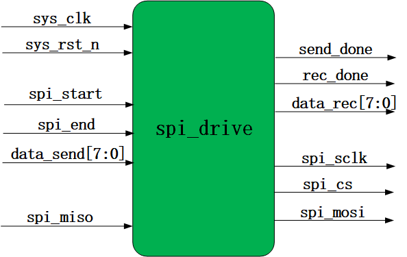
The signal is described as follows:
The module can be used as follows:
- Pull up SPI transmission start signal spi_start a cycle while sending data to data_send, the module sends the completion flag when the data is sent send_done pulls up a period, marking a BYTE's data sent to the slave via the SPI bus
- Similarly, when receiving the completion flag rec_ When done is elevated by this module, it means that the host successfully receives a BTYE data from the host
- When the host wants to end the transmission, it can end the SPI signal spi_ If the end is increased by one period, the module will end the SPI transmission after sending the last module, which also means that if the SPI end signal is not ended, the SPI transmission will continue to proceed in order to achieve the SPI transmission of multiple BYTE s
3.2, Verilog code
Verilog code is not complex, and in conjunction with the SPI communication process shown in the following figure, the following points can be found:
- SCK is well suited for a 4-way clock with a system clock because it needs to be operated four times in a single SCK
- Send and receive data by shifting the generated SCK's up and down edges, respectively.
- Additionally, as you can see from the figure below, SPI drivers are well suited for writing using state machines and are interested in trying them yourself.
`timescale 1ns/1ns //Time Unit/Precision
// Mode 0
module spi_drive
(
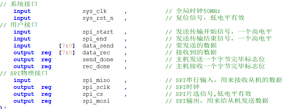
// system interface
input sys_clk , // Global clock 50MHz
input sys_rst_n , // Reset signal, low level effective
// User Interface
input spi_start , // Send transmission start signal, a high level
input spi_end , // Send end of transmission signal, a high level
input [7:0] data_send , // Data to send
output reg [7:0] data_rec , // Received data
output reg send_done , // Host sends a byte completion flag bit
output reg rec_done , // Host receives a byte completion flag bit
// SPI Physical Interface
input spi_miso , // SPI Serial Input to receive slave data
output reg spi_sclk , // SPI Clock
output reg spi_cs , // SPI Picture Selection Signal, Low Level Effective
output reg spi_mosi // SPI Output, used to send data to slaves
);
reg [1:0] cnt; //4-crossover counter
reg [3:0] bit_cnt_send; //Send Counter
reg [3:0] bit_cnt_rec; //Receive Counter
reg spi_end_req; //End Request
//4-crossover counter
always @(posedge sys_clk or negedge sys_rst_n)begin
if(!sys_rst_n)
cnt <= 2'd0;
else if(!spi_cs)begin
if(cnt == 2'd3)
cnt <= 2'd0;
else
cnt <= cnt + 1'b1;
end
else
cnt <= 2'd0;
end
// Generate spi_sclk clock
always @(posedge sys_clk or negedge sys_rst_n)begin
if(!sys_rst_n)
spi_sclk <= 1'b0; //Mode 0 defaults to low level
else if(!spi_cs)begin //During SPI transfer
if(cnt == 2'd0 )
spi_sclk <= 1'b0;
else if (cnt == 2'd2)
spi_sclk <= 1'b1;
else
spi_sclk <= spi_sclk;
end
else
spi_sclk <= 1'b0; //Mode 0 defaults to low level
end
// Generate Pick Signal spi_cs
always @(posedge sys_clk or negedge sys_rst_n)begin
if(!sys_rst_n)
spi_cs <= 1'b1; //Default to high level
else if(spi_start) //Start SPI ready for transmission, pull down the selected signal
spi_cs <= 1'b0;
//Received SPI end signal and ended the last BYTE
else if(spi_end_req && (cnt == 2'd1 && bit_cnt_rec == 4'd0))
spi_cs <= 1'b1; //Pull up the chip selection signal to end SPI transmission
end
// Generate end request signal (capture spi_end signal)
always @(posedge sys_clk or negedge sys_rst_n)begin
if(!sys_rst_n)
spi_end_req <= 1'b0; //Default not enabled
else if(spi_cs)
spi_end_req <= 1'b0; //Lower Request After Ending SPI Transfer
else if(spi_end)
spi_end_req <= 1'b1; //Raise the end request after receiving the SPI end signal
end
// Sending data process----------------------------------------------------------------------------------------------------------------------------------------------------------------------
// send data
always @(posedge sys_clk or negedge sys_rst_n)begin
if(!sys_rst_n)begin
spi_mosi <= 1'b0; //Mode 0 idle
bit_cnt_send <= 4'd0;
end
else if(cnt == 2'd0 && !spi_cs)begin //Rising edge of mode 0
spi_mosi <= data_send[7-bit_cnt_send]; //Send Data Shift
if(bit_cnt_send == 4'd7) //Send 8bit
bit_cnt_send <= 4'd0;
else
bit_cnt_send <= bit_cnt_send + 1'b1;
end
else if(spi_cs)begin //Non-transmission period
spi_mosi <= 1'b0; //Mode 0 idle
bit_cnt_send <= 4'd0;
end
else begin
spi_mosi <= spi_mosi;
bit_cnt_send <= bit_cnt_send;
end
end
// Send Data Flag
always @(posedge sys_clk or negedge sys_rst_n)begin
if(!sys_rst_n)
send_done <= 1'b0;
else if(cnt == 2'd0 && bit_cnt_send == 4'd7) //8bit data sent
send_done <= 1'b1; //Pull up a period to indicate that the send is complete
else
send_done <= 1'b0;
end
// Receiving data process--------------------------------------------------------------------------------------------------------------------------------------------------------------------
// Receive data spi_miso
always @(posedge sys_clk or negedge sys_rst_n)begin
if(!sys_rst_n)begin
data_rec <= 8'd0;
bit_cnt_rec <= 4'd0;
end
else if(cnt == 2'd2 && !spi_cs)begin //Rising edge of mode 0
data_rec[7-bit_cnt_rec] <= spi_miso; //Shift reception
if(bit_cnt_rec == 4'd7) //8bit received
bit_cnt_rec <= 4'd0;
else
bit_cnt_rec <= bit_cnt_rec + 1'b1;
end
else if(spi_cs)begin
bit_cnt_rec <= 4'd0;
end
else begin
data_rec <= data_rec;
bit_cnt_rec <= bit_cnt_rec;
end
end
// Receive Data Flag
always @(posedge sys_clk or negedge sys_rst_n)begin
if(!sys_rst_n)
rec_done <= 1'b0;
else if(cnt == 2'd2 && bit_cnt_rec == 4'd7) //8bit received
rec_done <= 1'b1; //Pull up a period to indicate that reception is complete
else
rec_done <= 1'b0;
end
endmodule4. Testbench and simulation results
4.1. Simulations of Single BYTE
Using this SPI driver, send a single BYTE data 8'b010101 to the slave machine to see if the simulation sequence is correct:
//------------------------------------------------
//--SPI driver simulation (mode 0, 1 BYTE)
//------------------------------------------------
`timescale 1ns/1ns		//Time Unit/Precision

//----------------<Module and Port Statement>--------------------------------------------------------------------------------------------------------------------------------
module tb_spi_drive();
//system interface
reg				sys_clk		;			// Global clock 50MHz
reg				sys_rst_n	;   		// Reset signal, low level effective
//User Interface
reg				spi_start 	;   		// Send transmission start signal, a high level
reg				spi_end   	;   		// Send end of transmission signal, a high level
reg		[7:0]  	data_send   ;   		// Data to send
wire  	[7:0]  	data_rec  	;   		// Received data
wire         	send_done	;   		// Host sends a byte completion flag bit
wire         	rec_done	;   		// Host receives a byte completion flag bit
//SPI Physical Interface
reg				spi_miso	;   		// SPI Serial Input to receive slave data
wire         	spi_sclk	;   		// SPI Clock
wire			spi_cs    	;   		// SPI Picture Selection Signal
wire         	spi_mosi	;   		// SPI Output, used to send data to slaves
//Simulation
reg		[3:0]  	cnt_send 	;			//Send Data Counter, 0-15

//-------------- <instantiated SPI driver module (mode 0)>--------------------------------------------------------------------------------------------------------------------------------------
spi_drive	spi_drive_inst(
	.sys_clk		(sys_clk	),
	.sys_rst_n		(sys_rst_n	),

	.spi_start		(spi_start	),
	.spi_end		(spi_end	),
	.data_send		(data_send	),
	.data_rec  		(data_rec	),
	.send_done		(send_done	),
	.rec_done		(rec_done	),

	.spi_miso		(spi_miso	),
	.spi_sclk		(spi_sclk	),
	.spi_cs    		(spi_cs		),
	.spi_mosi		(spi_mosi	)
);

//---------------- <Set Initial Test Conditions>----------------------------------------------------------------------------------------------------------------------------
initial begin
	sys_clk = 1'b0;						//Initial clock is 0
	sys_rst_n <= 1'b0;					//Initial Reset
	spi_start <= 1'b0;
	data_send <= 8'd0;
	spi_miso <= 1'bz;
	spi_end <= 1'b0;
	#80 									// After 80 Clock Cycles
	sys_rst_n <= 1'b1;					//Pull up and reset the system to work
	#30 									// Pull up the SPI start signal after 30 clock cycles to start SPI transmission
	spi_start <= 1'b1;data_send <= 8'b01010101;
	#20
	spi_start <= 1'b0;
	@(posedge send_done)				//A BYTE send is complete
	spi_end <= 1'b1;	#20 	 Spi_ End <= 1'b0; 	// Pull up the cycle end signal

end

//------------------------------------------------------------------------------------------------------------------------------------------------------------------------
always #10 sys_clk = ~sys_clk; 					// System clock cycle 20ns

endmodule
The simulation results are as follows:
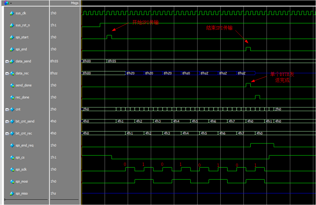
As you can see, spi_is being pulled up After start starts transmitting the signal, the host starts sending data. The data on the MOSI is 010101. After sending a BYTE, send_done pulls up. Pull up the end signal spi_at this time End, the SPI transfer is terminated, and the SPI transfer of a single BYTE is completed.
4.2, Simulation of Multiple BYTE s
Using this SPI driver, send data 8'd0~8'd10 from the slave machine in turn to see if the simulation sequence is correct:
//------------------------------------------------
//--SPI Drive Simulation (Mode 0)
//------------------------------------------------
`timescale 1ns/1ns		//Time Unit/Precision

//----------------<Module and Port Statement>--------------------------------------------------------------------------------------------------------------------------------
module tb_spi_drive();
//system interface
reg				sys_clk		;			// Global clock 50MHz
reg				sys_rst_n	;   		// Reset signal, low level effective
//User Interface
reg				spi_start 	;   		// Send transmission start signal, a high level
reg				spi_end   	;   		// Send end of transmission signal, a high level
reg		[7:0]  	data_send   ;   		// Data to send
wire  	[7:0]  	data_rec  	;   		// Received data
wire         	send_done	;   		// Host sends a byte completion flag bit
wire         	rec_done	;   		// Host receives a byte completion flag bit
//SPI Physical Interface
reg				spi_miso	;   		// SPI Serial Input to receive slave data
wire         	spi_sclk	;   		// SPI Clock
wire			spi_cs    	;   		// SPI Picture Selection Signal
wire         	spi_mosi	;   		// SPI Output, used to send data to slaves
//Simulation
reg		[3:0]  	cnt_send 	;			//Send Data Counter, 0-15

//-------------- <instantiated SPI driver module (mode 0)>--------------------------------------------------------------------------------------------------------------------------------------
spi_drive	spi_drive_inst(
	.sys_clk		(sys_clk	),
	.sys_rst_n		(sys_rst_n	),

	.spi_start		(spi_start	),
	.spi_end		(spi_end	),
	.data_send		(data_send	),
	.data_rec  		(data_rec	),
	.send_done		(send_done	),
	.rec_done		(rec_done	),

	.spi_miso		(spi_miso	),
	.spi_sclk		(spi_sclk	),
	.spi_cs    		(spi_cs		),
	.spi_mosi		(spi_mosi	)
);

//---------------- <Set Initial Test Conditions>----------------------------------------------------------------------------------------------------------------------------
initial begin
	sys_clk = 1'b0;						//Initial clock is 0
	sys_rst_n <= 1'b0;					//Initial Reset
	spi_start <= 1'b0;
	data_send <= 8'd0;
	spi_miso <= 1'bz;
	spi_end <= 1'b0;
	#80 									// After 80 Clock Cycles
	sys_rst_n <= 1'b1;					//Pull up and reset the system to work
	#30 									// Pull up the SPI start signal after 30 clock cycles to start SPI transmission
	spi_start <= 1'b1;	#20	spi_start <= 1'b0;
end

always@(posedge sys_clk or negedge sys_rst_n)begin
	if(!sys_rst_n)begin
		data_send <= 8'd0;
		spi_end <= 1'b0;
		cnt_send <= 4'd0;
	end
	else if(send_done)begin						//Data Send Complete
		if(cnt_send == 4'd10)begin
			cnt_send <= 4'd0;
			spi_end <= 1'b1;					//Pull up the end flag to end the SPI transfer process
			data_send <= 8'd0;
		end
		else begin
			cnt_send <= cnt_send + 4'd1;
			spi_end <= 1'b0;
			data_send <= data_send + 4'd1;		//Send Data Accumulation
		end
	end
	else begin
		data_send <= data_send;
		spi_end <= 1'b0;						//Keep SPI transmission on other occasions (do not end)
	end
end

//------------------------------------------------------------------------------------------------------------------------------------------------------------------------
always #10 sys_clk = ~sys_clk; 					// System clock cycle 20ns

endmodule
The simulation results are as follows:
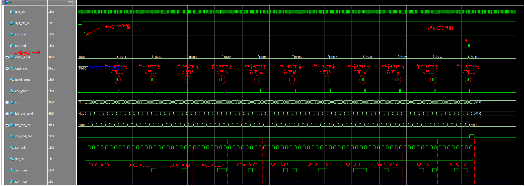
As you can see, spi_is being pulled up The host has been sending data since start started transmitting signal. The data on the MOSI is 8'd0~8'd10. After sending one BYTE data at a time, send_done pulls up once. When the end signal spi_ When the end is raised, the SPI transmission is terminated.
5. Other
- It is important to note that since there is no offline response, MISO s are all high resistance (blue)
- Next article combines slave machine (FLASH chip) to simulate and verify receiving data function
- Friends who want the whole project can leave their mailbox in the comments area